Introduction to Nanotechnology
The nanoscale world, its pioneers, and the foundational approaches to building with matter at its most fundamental level.
Contents
- What is the Nanoscale?
- The Human Body — A Nano Machine
- Nature as the Original Nanotechnologist
- A Brief History: Feynman, Taniguchi & Drexler
- Photosynthesis — Nature's Nanoscale Factory
- What Makes Nanotechnology Special?
- Challenges & Skeptical Questions
- Top-Down vs. Bottom-Up Fabrication
- Photolithography — The Workhorse of Top-Down
- Key Takeaways
1 What is the Nanoscale?
The prefix nano derives from the Greek word for "dwarf," and in scientific notation it represents one billionth — 10−9. A nanometre (nm) is therefore one billionth of a metre. To appreciate just how small this is, consider that a human hair is roughly 80,000 nm wide, a single red blood cell measures about 7,000 nm across, and a DNA double helix has a diameter of only 2 nm. The nanoscale sits at the very boundary between individual atoms and molecules on one side, and the macroscopic world we interact with daily on the other.
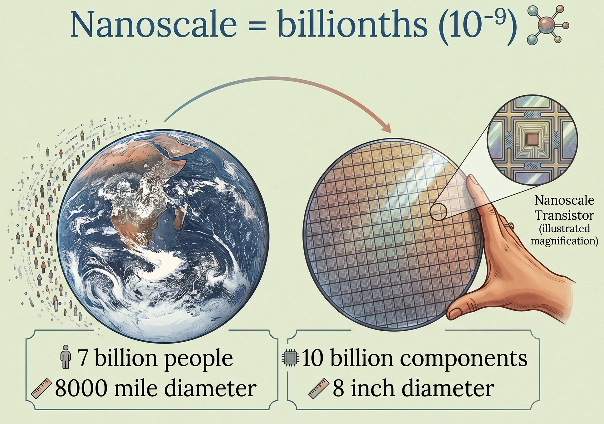
The comparison between the Earth and a silicon wafer is deeply instructive. A modern semiconductor chip packs more functional elements into a palm-sized object than there are people on our entire planet. This is only possible because those elements operate at nanometre dimensions — and understanding why matter behaves differently at that scale is the central question of nanoscience.
When material dimensions shrink to the nanometre range, two dramatic changes occur: (1) the surface-to-volume ratio becomes enormous, altering chemical reactivity and thermodynamic stability; and (2) quantum mechanical effects begin to dominate electronic, optical, and magnetic behaviour. Classical physics simply cannot describe these phenomena accurately.
2 The Human Body — A Nano Machine
One of the most compelling arguments for the relevance of nanoscience is the human body itself. A 70 kg adult is composed of approximately 6.71 × 1027 atoms — a number so vast it is essentially incomprehensible. Hydrogen, oxygen, carbon, and nitrogen together account for over 99% of all atoms by number, yet tens of other elements are present in smaller quantities, each playing precise biochemical roles.
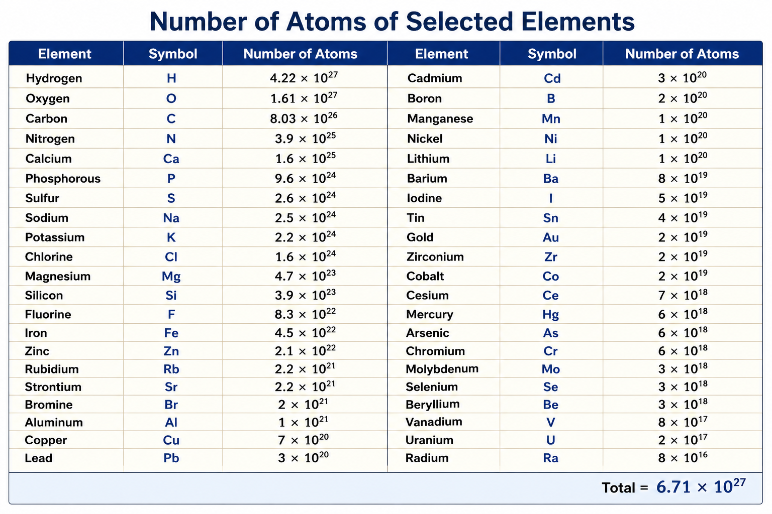
What is remarkable is not just the sheer number of atoms, but the extraordinary precision with which they are arranged. A haemoglobin molecule — responsible for oxygen transport — is about 5.5 nm across. The ion channels embedded in neural membranes that enable thought are gated at the single-molecule level. Life, viewed through this lens, is a demonstration of what is possible when atoms are arranged with nanoscale precision.
If the raw atoms in a human body were purchased as chemical elements, the cost would be roughly equivalent to a good pair of shoes. Yet those same atoms, arranged with nanoscale precision by biological processes, constitute a thinking, breathing, self-repairing organism of immeasurable complexity. The arrangement is everything — and that is the central promise of nanotechnology.
3 Nature as the Original Nanotechnologist
Long before human engineers began to dream of manipulating matter at the nanoscale, nature had perfected it. Biological systems operate across an enormous range of length scales — from the sub-nanometre world of individual atoms and bonds, through the nanoscale realm of DNA, proteins, and viruses, all the way up to macroscopic organisms like blue whales measuring over 30 metres.
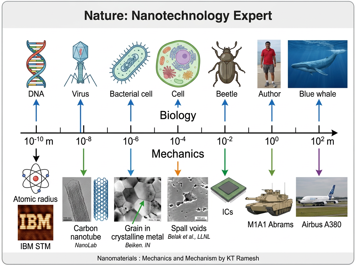
This length-scale diagram makes two things immediately apparent. First, biological materials have been operating at the nanoscale for billions of years — evolution is, in a very real sense, the world's longest-running nanotechnology programme. Second, the engineering structures we build span a remarkably similar range of scales. The convergence of biology-inspired design with engineering ambition is one of the defining features of modern nanotechnology.
The concept that matter can be arranged atom by atom to achieve desired functions was inspired directly by observing nature. The human body assembles itself from a single fertilised cell through molecular instructions encoded in DNA, self-organising into ~37 trillion cells with extraordinary precision. Biomimicry — deliberately designing materials and devices that imitate natural nanotechnology — is now one of the most active research directions in the field.
4 A Brief History: Feynman, Taniguchi & Drexler
Although nanotechnology as a formal discipline is relatively young, its intellectual roots go back more than six decades. Three figures stand out as foundational.
On 29th December 1959, Feynman asked a question that seemed almost absurd at the time: what would happen if we could arrange individual atoms exactly where we wanted them? He pointed out there was no fundamental physical law preventing this — only a lack of the right tools. He challenged the audience to build a functioning electric motor inside a cube 1/64th of an inch on a side, and to write the entire Encyclopaedia Britannica on the head of a pin. Both challenges were eventually met. Feynman's lecture gave nanotechnology an intellectual pedigree connected to one of the towering figures of 20th-century physics.
Norio Taniguchi of Tokyo University of Science formally used "nano-technology" for the first time in a 1974 conference paper, describing semiconductor fabrication processes — thin-film deposition, ion-beam milling — that achieved control on the order of a nanometre. This perspective — starting with bulk material and shaping it to produce nanoscale features — is what we now call the top-down approach.
Drexler encountered Feynman's talk in 1980 and published his first molecular engineering paper in PNAS in 1981. His 1986 book Engines of Creation proposed molecular assemblers: nanoscale machines capable of precisely placing individual atoms to build any desired structure, including copies of themselves. This vision, called Molecular Nanotechnology (MNT), remains both inspiring and scientifically debated.
5 Photosynthesis — Nature's Nanoscale Factory
Among the many examples of nature's mastery of nanotechnology, photosynthesis is arguably the most instructive and the most elegant. It is a process of such extraordinary efficiency that human engineers have spent decades trying to understand and replicate it — so far with only partial success.
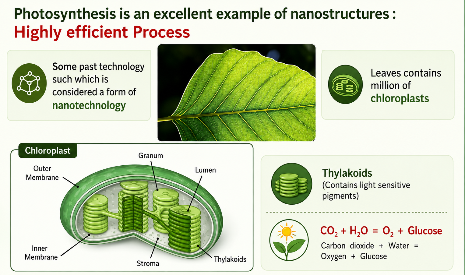
The architecture of the chloroplast is a masterclass in nanoscale engineering. Each granum consists of disc-like thylakoid membranes stacked like coins, with diameters typically in the 200–600 nm range. Within the thylakoid, Light Harvesting Complex II (LHCII) acts as an antenna array that absorbs photons across a broad range of wavelengths and transfers excitation energy to Photosystem II with quantum efficiencies approaching 95–99%. Quantum coherence — a purely quantum mechanical phenomenon — is thought to play a role in this energy transfer, making the chloroplast one of the few biological systems known to exploit quantum effects at physiological temperatures.
Photosynthesis evolved approximately 3.4 billion years ago. The light-harvesting complexes are self-assembled nanoscale protein machines — synthesised, folded, and inserted into the membrane without any external guidance, driven entirely by thermodynamics and genetic information. Nature had mastered bottom-up nanofabrication long before the word "nanotechnology" was coined.
6 What Makes Nanotechnology Special?
Nanotechnology does not belong to any single discipline — it sits at the intersection of physics, chemistry, materials science, biology, electrical engineering, and medicine. A researcher working on drug delivery nanoparticles needs knowledge of surface chemistry, polymer science, cell biology, and pharmacokinetics simultaneously. This interdisciplinarity is one of the reasons nanotechnology has grown so rapidly — insights from one field constantly catalyse breakthroughs in another.
At the nanoscale, materials inhabit a transitional regime — too large to be described fully by quantum chemistry for isolated atoms, yet too small to behave like bulk materials. In this intermediate regime, properties can change dramatically and non-linearly with size. Gold is chemically inert in bulk form. Gold nanoparticles of 3–5 nm diameter, however, are highly active catalysts capable of oxidising carbon monoxide at room temperature. The colour also shifts with size: 20 nm particles appear red, 80 nm particles appear orange, and larger particles approach the familiar yellow of bulk gold. Same element, entirely different behaviour — purely because of size.
The lecture characterises nanotechnology as "one of the final great challenges" — the quest to achieve full control over materials at the atomic scale. If we could place every atom exactly where we wanted it, we could manufacture materials of perfect purity, devices of perfect functionality, and medicines that interact with the body at the molecular level. Achieving this level of control at scale, with reliability and at reasonable cost, remains an enormous unsolved problem that defines the frontier of materials science.
A 1 cm iron cube has a surface area of 6 cm². Divide it into 1 nm nanocubes and the combined surface area becomes 6 × 107 cm² — an increase of seven orders of magnitude. Since chemical reactions and catalysis occur at surfaces, this explains why nanomaterials are so much more reactive and chemically distinct from their bulk counterparts.
7 Challenges & Skeptical Questions
Despite the excitement surrounding nanotechnology, the field faces genuine scientific and engineering challenges that any serious student must engage with honestly.
Individual atoms and molecules are subject to thermal vibrations at any temperature above absolute zero. Can nanoscale devices maintain structural integrity in the face of these incessant vibrations? The answer depends on the specific system: covalently bonded structures like diamond or carbon nanotubes are extremely robust, while weakly bonded assemblies may be fragile. Biology again provides encouragement — proteins and DNA maintain functional three-dimensional structures in the warm, wet, thermally noisy environment of the living cell.
Quantum mechanics introduces tunnelling, uncertainty, and wave-particle duality — phenomena with no classical analogues. At the nanoscale, electrons can tunnel through energy barriers, causing leakage currents that have become a major limitation in transistor scaling. However, quantum effects are not always obstacles. Quantum dots exploit quantum confinement for highly tunable optical emission. Quantum tunnelling is the operating principle of the STM. The challenge is to design nanosystems that either avoid problematic quantum effects or harness beneficial ones.
Brownian motion — the random thermal buffeting of nanoscale particles by surrounding solvent molecules — makes directed motion difficult at the nanoscale. This is why nanoscale drug delivery vehicles require surface functionalisation to target specific cells rather than diffusing randomly. Nature has solved this elegantly: molecular motors like kinesin walk directionally along microtubule tracks despite constant Brownian bombardment, using chemical energy to maintain directionality.
At the nanoscale, adhesion forces become comparable to or larger than gravitational forces, and wear can occur through single-atom removal events. Understanding tribology at the nanoscale is critical for designing reliable nanomechanical systems and long-term stability of nanotextured surfaces — challenges that macroscale engineering has no direct precedent for.
These questions are not reasons to abandon nanotechnology — they are the research agenda that drives the field forward. Many barriers identified in the 1990s have since been substantially addressed through sustained experimental and theoretical work. The skepticism is healthy and productive.
8 Top-Down vs. Bottom-Up Fabrication
In top-down fabrication, one begins with a bulk material and progressively removes or shapes material to produce smaller and smaller features — like a sculptor revealing a form by removing marble. The dominant technique is lithography, supplemented by deposition (CVD, PVD) and etching. The key advantage is integration with existing manufacturing: parts are patterned and built in place, so no separate assembly step is needed. Modern semiconductor foundries produce billions of identical transistors per wafer with extraordinary reliability using this philosophy.
In the bottom-up approach, individual atoms, molecules, or nanoscale building blocks are assembled into larger structures — precisely what biology does. Examples include the growth of quantum dots from molecular precursors in solution, self-assembly of block copolymers into periodic patterns, and directed assembly of DNA origami structures. Bottom-up can achieve atomic precision and can produce 3D structures top-down methods struggle with, but scaling to industrial volumes remains a significant engineering challenge.
The most powerful nanofabrication strategies combine both approaches. Top-down lithography defines macro-architecture and interconnects; bottom-up self-assembly fills in nanoscale details lithography cannot resolve. Directed self-assembly (DSA), which uses lithographically defined templates to guide block copolymer self-organisation, is already being explored by semiconductor manufacturers for sub-10 nm patterning.
9 Photolithography — The Workhorse of Top-Down
Photolithography uses light to transfer a pattern from a mask to a photosensitive material (photoresist) coated on a substrate, enabling the parallel production of billions of identical nanoscale features. It is the foundational technique of the entire semiconductor industry, forming the backbone of every modern chip, from microprocessors to memory modules.
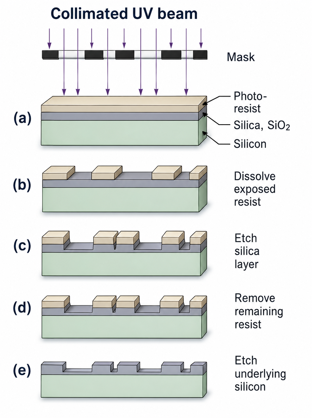
The process begins with a silicon wafer that has been thermally oxidised to grow a thin layer of silicon dioxide (SiO₂) on its surface. A liquid photoresist — a light-sensitive polymer — is then spin-coated onto the wafer to a precisely controlled thickness, typically 100–500 nm. The coated wafer is placed beneath a photomask: a glass plate on which a circuit pattern has been etched into an opaque chrome film. A collimated beam of ultraviolet light is then directed through the mask. Where the UV passes through transparent regions of the mask, it causes a photochemical reaction in the resist below.
In a positive photoresist, UV exposure breaks chemical bonds in the polymer, making the exposed regions soluble in a developer solution — these areas are washed away, leaving behind a negative image of the mask. In a negative photoresist, UV exposure causes cross-linking, making exposed regions insoluble while the unexposed areas wash away, leaving a positive image. The resulting patterned resist layer acts as an etch mask for subsequent steps: wet chemical etching or dry plasma etching then transfers the pattern into the underlying SiO₂ or silicon. After etching, the photoresist is stripped using solvents or oxygen plasma, and the cycle can begin again with a new mask layer. A complete modern integrated circuit may require 50–100 such lithography-etch cycles, each adding a new level of pattern complexity.
Despite its industrial dominance, photolithography faces both fundamental physical and severe practical limitations as feature dimensions shrink toward and below 10 nm.
The diffraction limit: The minimum resolvable feature size in photolithography is governed by the Rayleigh criterion: R = kλ/NA, where λ is the wavelength of the exposing light, NA is the numerical aperture of the projection lens, and k is a process-dependent factor (typically 0.25–0.5). Conventional deep-ultraviolet (DUV) sources use light at 193 nm wavelength. Even with aggressive optical tricks — immersion lithography (filling the gap between lens and wafer with water to increase NA), phase-shift masks, and off-axis illumination — features much smaller than ~40 nm are extremely difficult to resolve. To print the sub-10 nm features of advanced logic nodes, the industry has moved to Extreme Ultraviolet (EUV) lithography, which uses light at 13.5 nm — generated by directing high-power laser pulses onto tiny tin droplets to produce a plasma that emits EUV radiation. EUV enables ~13 nm half-pitch resolution in a single exposure, but the technology required decades to bring to manufacturing readiness.
Mask alignment and overlay: A modern integrated circuit contains multiple layers of patterns, each of which must align with the layer below to within a fraction of the minimum feature size. At 3 nm process nodes, overlay tolerances are measured in single-digit nanometres across a 300 mm wafer — a feat analogous to aligning two dinner plates placed on opposite sides of a football field to within the width of a human hair. Achieving this requires active vibration isolation, precision interferometric stage metrology, machine learning-based distortion correction, and increasingly sophisticated alignment mark designs.
Defect density control: Even a single airborne particle of dust landing on a mask or wafer surface can create a defect that destroys many devices. Photolithography must therefore be performed in Class 1 or Class 10 cleanrooms — environments where the number of particles larger than 0.1 µm per cubic foot of air is controlled to 1 or 10, respectively. By comparison, a typical office building contains roughly 1,000,000 such particles per cubic foot. Maintaining cleanroom conditions requires sophisticated HEPA filtration, positive-pressure air handling, strict gowning protocols, and continuous particle monitoring. Mask inspection and repair have themselves become billion-dollar industries.
Stochastic effects at EUV wavelengths: At EUV wavelengths, the number of photons available per feature area becomes small enough that statistical fluctuations — shot noise — begin to cause random line-edge roughness and feature-to-feature variability. This quantum-mechanical effect has no classical analogue and sets a fundamental floor on how perfect EUV-patterned features can be, regardless of how good the optics are. Managing stochastic effects is now one of the central research challenges in advanced lithography.
Cost: A single state-of-the-art EUV lithography system (manufactured exclusively by ASML in the Netherlands) costs approximately US50–350 million, depending on the generation. The entire infrastructure for a leading-edge semiconductor fab — cleanrooms, process equipment, metrology, yield management — typically costs US5–25 billion. This enormous capital intensity means that advanced semiconductor manufacturing is now concentrated in fewer than five companies globally, and that any disruption to this supply chain — whether geopolitical, natural disaster, or technical — has immediate consequences for the global electronics industry.
Gordon Moore's 1965 observation — that the number of transistors on an integrated circuit roughly doubles every two years — has held for over six decades, enabled entirely by continuous improvements in photolithography. The transistors in current 3 nm process nodes (the naming is now largely marketing — actual gate lengths are closer to 12–18 nm) are assembled from structures only a handful of atoms across in their critical dimensions. We are approaching the physical limits of silicon-based top-down fabrication, which is one of the most powerful industrial drivers of interest in alternative bottom-up and hybrid nanofabrication strategies — and why nanoscience as a field has never been more important to the global economy.
Key Takeaways
- The nanoscale (1–100 nm) is a regime where materials exhibit qualitatively different properties from both isolated atoms and bulk matter, driven by quantum confinement and dramatically increased surface-to-volume ratios.
- The human body — assembled atom by atom through biological processes — is a compelling existence proof of nanoscale precision engineering.
- Feynman (1959) provided the conceptual foundation; Taniguchi (1974) coined the term; Drexler (1981/86) articulated the bottom-up vision. All three were necessary for the field to take shape.
- Photosynthesis is the canonical example of nature's nanotechnology — a self-assembled, quantum-efficient solar energy conversion system operating within nanometre-scale thylakoid membranes.
- Top-down (remove material) and bottom-up (build up from atoms) fabrication philosophies are complementary; the future lies in their intelligent integration.
- Photolithography dominates semiconductor manufacturing but faces the diffraction limit, stochastic noise, extreme cost, and overlay challenges as features shrink below 10 nm.
- Genuine challenges — thermal stability, quantum effects, Brownian motion, nanoscale tribology — define the active research frontier and are not reasons for pessimism.
✦ References & Further Reading
- Guozhong Cao, Nanostructures & Nanomaterials: Synthesis, Properties and Applications, Imperial College Press, 2nd Ed.
- H. S. Nalwa (Ed.), Handbook of Nanostructured Materials and Nanotechnology, Vols 1–5, Academic Press, 2000.
- Poole and Owens, Introduction to Nanotechnology, Wiley.
- T. Pradeep, Nano — The Essentials.
- Ashby, Ferreira, Schodek, Nanomaterials, Nanotechnologies and Design, BH Press, Oxford, 2009.
- Murty et al., Textbook of Nanoscience and Nanotechnology, Universities Press–IIM.
Nanofabrication: Top-Down & Bottom-Up Approaches
From photolithography and plasma etching to self-assembly and atomic-layer deposition — the strategies engineers use to build structures at the nanoscale, and how dimensionality shapes what we call a nanomaterial.
Contents
- Why We Need New Fabrication Strategies
- Photolithography — Printing Patterns with Light
- Positive and Negative Photoresists
- Atomic Manipulation — The Bottom-Up Extreme
- Making Nanostructures — The Fabrication Toolkit
- Deposition — Building Films from the Vapour Phase
- Etching — Sculpting Matter by Selective Removal
- Micromachining & CVD vs. PVD
- Self-Assembly — Order from Molecular Forces
- Classifying Nanomaterials — Dimensionality
- Characterising Nanomaterials by Dimensionality
- References & Further Reading
1 Why We Need New Fabrication Strategies
The driving force behind every new generation of nanotechnology is a deceptively simple ambition: to create materials and devices whose properties exceed what is achievable through conventional microstructural engineering. The twentieth century saw remarkable progress along what might be called the classical route — controlling grain size and defect populations through thermomechanical processing, using theory of dislocations and defects to understand mechanical behaviour, and exploiting structure–property relationships to produce stronger, lighter, and more functional materials. Tools like the transmission electron microscope (TEM) and the field-ion microscope (FIM) made it possible to see and interpret microstructure at ever finer length scales. But as device dimensions cross below the micrometre threshold, a qualitatively different kind of fabrication is required.
The central challenge of nanofabrication is precision at a scale where individual atoms matter. Two philosophically distinct strategies have emerged. The top-down approach begins with a bulk material and progressively patterns or removes material — sculpting nanoscale features from the macroscale downward, much as a sculptor reveals a form by removing stone. The bottom-up approach begins with individual atoms or molecules and builds ordered complexity upward through directed assembly or spontaneous self-organisation. In practice, the most powerful technologies blend both: top-down templates guide bottom-up assembly, and bottom-up films are patterned by top-down lithography.
The central lesson of materials science — that microstructure determines properties — becomes extreme at the nanoscale. A 5 nm gold nanoparticle catalyses reactions that bulk gold cannot. A graphene monolayer conducts electricity faster than any metal. A carbon nanotube surpasses steel in tensile strength. In every case, the dramatic property change emerges not from a different chemical composition, but from a different spatial arrangement of the same atoms. Controlling that arrangement with atomic precision is the goal of nanofabrication.
2 Photolithography — Printing Patterns with Light
Photolithography is the cornerstone of semiconductor manufacturing and the most widely deployed top-down nanofabrication technique in existence. The fundamental idea is elegant: use light to transfer a geometric pattern from a master template (the mask) onto the surface of a substrate coated with a light-sensitive polymer (the photoresist). By selectively exposing regions of the resist and then chemically developing it, a stencil is created that allows subsequent etching or deposition steps to modify the underlying material with spatial precision.
The substrate — typically a silicon wafer — is first cleaned and thermally oxidised to produce a surface layer of silicon dioxide (SiO₂). A photoresist film, spun onto the wafer at a precisely controlled thickness, is then applied. The mask — a quartz plate carrying an opaque chromium pattern — is aligned over the wafer and a collimated UV beam is projected through it. Wherever light passes through the transparent regions, the resist undergoes a chemical change. The wafer is then developed: the chemically altered regions are dissolved away, and what remains is a patterned polymer stencil that guides all subsequent processing.
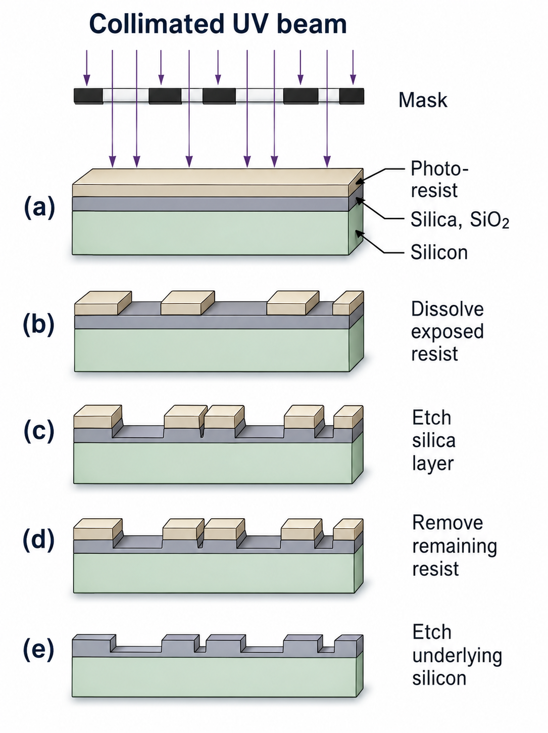
The resolution limit of photolithography is set by the diffraction of light. The Rayleigh criterion gives the minimum resolvable feature as approximately λ/(2·NA), where λ is the illumination wavelength and NA is the numerical aperture of the lens system. This relationship drove decades of wavelength reduction: from visible mercury lamp emission (436 nm g-line, 365 nm i-line) to deep ultraviolet excimer lasers (248 nm KrF, then 193 nm ArF), and most recently to extreme ultraviolet (EUV) at 13.5 nm — a wavelength produced not by a lamp but by a tin plasma bombarded with high-power lasers. Modern EUV systems, combined with multiple-patterning techniques and optical proximity correction, enable the definition of features below 5 nm — transistor gate lengths that are only about 20 silicon atoms wide.
3 Positive and Negative Photoresists
A critical design choice in any lithographic process is the type of photoresist. Positive and negative resists respond to radiation in chemically opposite ways, and this difference produces complementary pattern geometries from the same mask. Understanding the distinction is essential for choosing the right resist for a given application.
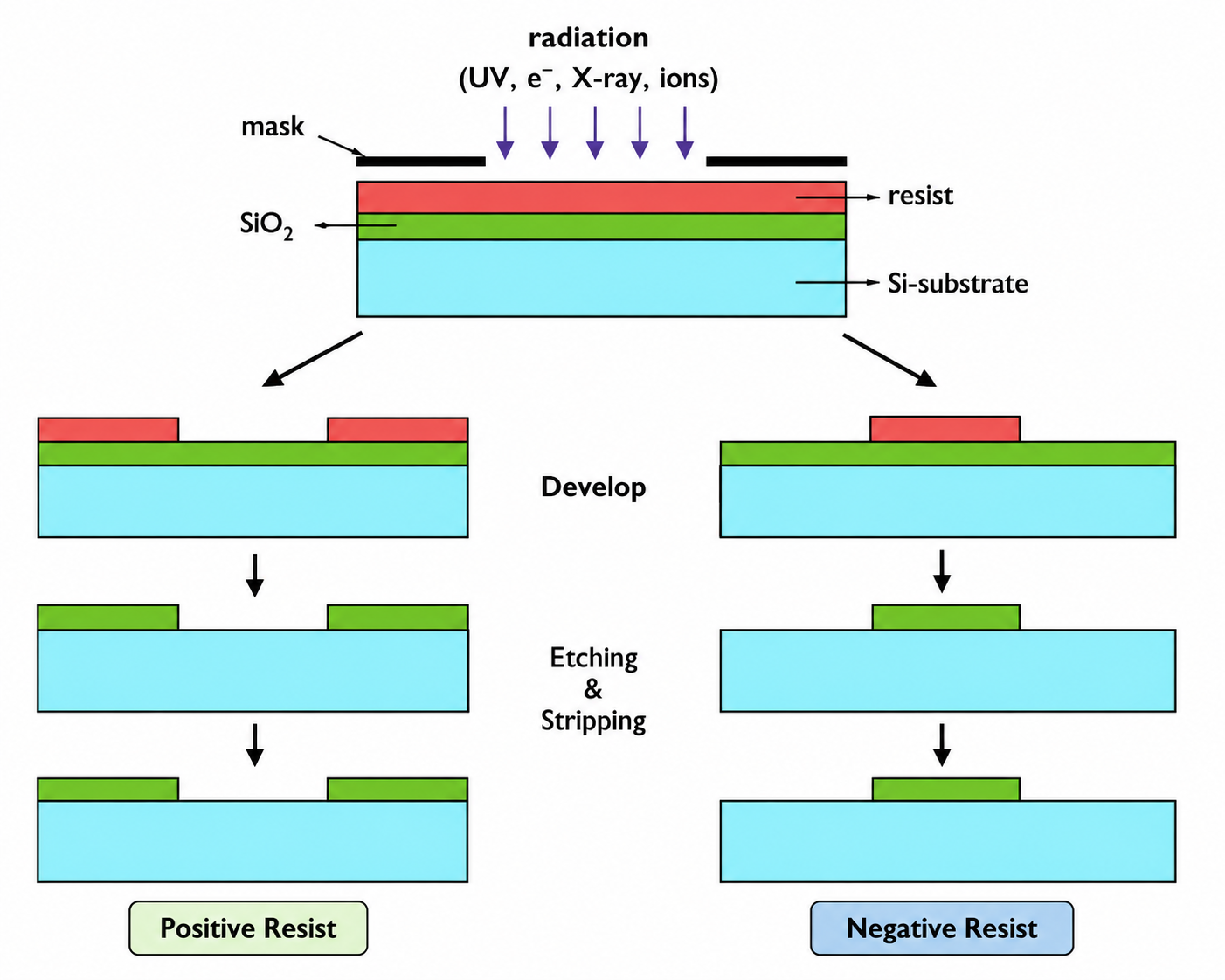
In a positive photoresist, exposure causes chain scission — the long polymer chains that give the resist its mechanical integrity are broken into shorter, more soluble fragments. Illuminated regions dissolve away in the developer, leaving resist intact only in the shadowed areas. Positive resists are the dominant choice in sub-micrometre patterning because the dissolution contrast between exposed and unexposed regions is very sharp, and there is minimal swelling during development — swelling blurs feature edges and is a primary resolution-limiting artefact of negative resists.
In a negative photoresist, irradiation induces cross-linking between adjacent polymer chains, creating a dense network that is insoluble in the developer. The unexposed regions remain as short, soluble chains and wash away. Negative resists offer higher photosensitivity — less light dose is needed to expose them — and they adhere exceptionally well to the substrate after exposure, making them preferred for lift-off patterning processes. However, the physical swelling accompanying cross-link formation distorts feature edges, and pattern collapse becomes a risk as features are scaled below 100 nm.
Both positive and negative resists can be formulated for radiation sources other than UV light. Electron-beam (e-beam) lithography uses a tightly focused beam of electrons to expose the resist, bypassing the diffraction limit entirely — electrons at typical accelerating voltages (10–100 kV) have de Broglie wavelengths of picometres, far smaller than any optical wavelength. E-beam lithography can write features below 10 nm and is used for mask making and research-scale fabrication, but it exposes the wafer serially (one point at a time) rather than all at once, making it too slow for high-volume manufacturing. Focused ion beam (FIB) systems go further still — ions are massive enough to physically sputter material as well as expose resist, enabling direct maskless milling of nanoscale features.
4 Atomic Manipulation — The Bottom-Up Extreme
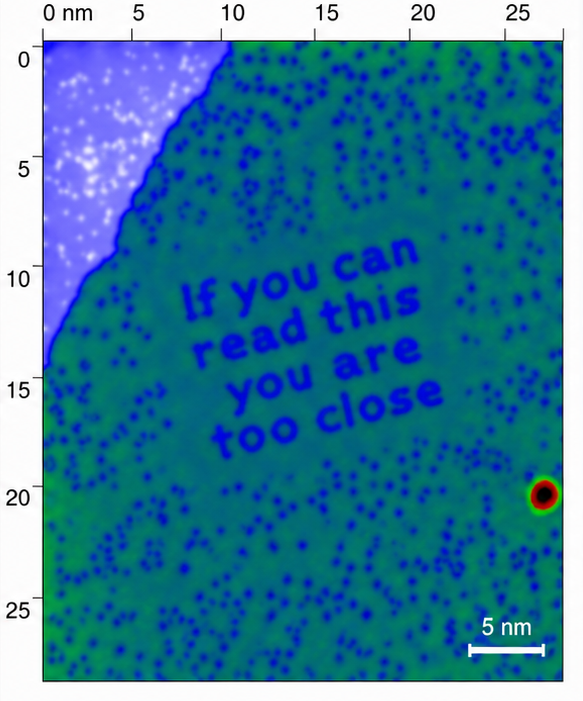
While photolithography defines patterns across entire wafers simultaneously, the most radical expression of the bottom-up vision involves positioning individual atoms one at a time to deliberately chosen locations on a surface. This capability was spectacularly demonstrated at IBM's Almaden Research Center, when Donald Eigler and Erhard Schweizer used a scanning tunnelling microscope (STM) to spell out the letters "IBM" using 35 xenon atoms on a nickel surface cooled to 4 K. The experiment was far more than a publicity gesture — it constituted the first definitive proof that individual atoms could be repositioned at will, establishing the experimental foundation for what Feynman had theorised decades earlier.

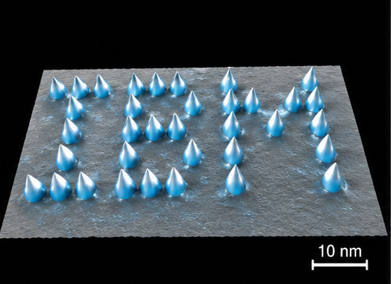
The STM operates by bringing an atomically sharp metal tip to within approximately 1 nm of a conducting surface and applying a small bias voltage. Quantum mechanical tunnelling drives a tiny electrical current — typically picoamperes — across the vacuum gap, decaying exponentially with distance. A feedback loop maintains constant tunnel current as the tip scans, mapping surface electronic topography with sub-ångström vertical resolution. To manipulate atoms, the tip is brought even closer, allowing van der Waals and short-range chemical forces to drag or push a target atom to a new lattice site. The process demands ultra-high vacuum, exceptional mechanical isolation from vibration, and cryogenic temperatures — at room temperature, adatoms diffuse too rapidly across the surface for static structures to survive.
A particularly vivid illustration of what becomes possible at this level of control was provided by IBM's Almaden group in a separate experiment — the "Fun With Atoms" image.
5 Making Nanostructures — The Fabrication Toolkit
Between the industrial-scale parallel processing of photolithography and the atomic-resolution precision of STM manipulation lies a rich and diverse toolkit of nanofabrication methods. The field organises these into four major top-down process families — lithography, deposition, etching, and micromachining — and two principal bottom-up approaches: CVD/PVD vapour-phase growth and self-assembly. No single method dominates; the choice always depends on the material system, required feature size, throughput, and cost constraints.
Top-down methods offer excellent spatial control and direct compatibility with existing semiconductor manufacturing infrastructure, but become physically harder and exponentially more expensive as feature sizes approach and cross below 10 nm — the regime where quantum mechanics dominates and surface effects make every atom count. Bottom-up methods can produce atomically precise structures naturally and cheaply, but struggle with achieving long-range positional order across a macroscopic device. The frontier of nanofabrication lies in combining both: top-down-defined templates guide bottom-up self-assembly into precisely specified locations, a strategy called directed self-assembly (DSA) that is already entering commercial semiconductor manufacturing.
6 Deposition — Building Films from the Vapour Phase
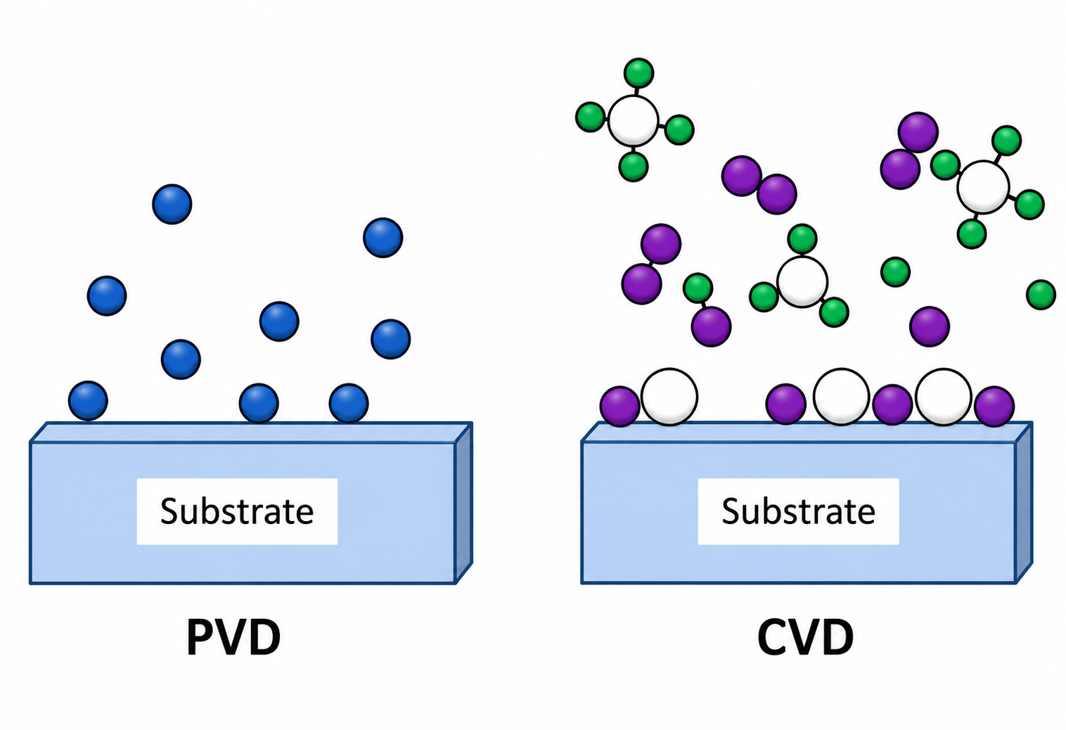
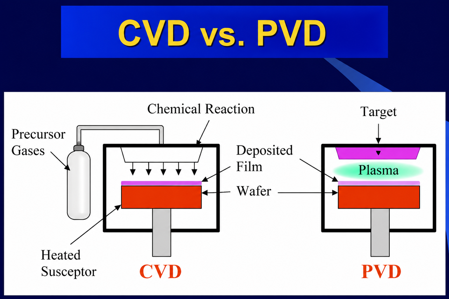
Deposition encompasses any process in which material is added to a substrate to build up a thin film or coating. The goal in nanofabrication is to control film thickness, composition, microstructure, and surface morphology with nanometre-level accuracy. The two dominant families — physical vapour deposition (PVD) and chemical vapour deposition (CVD) — achieve this through fundamentally different mechanisms.
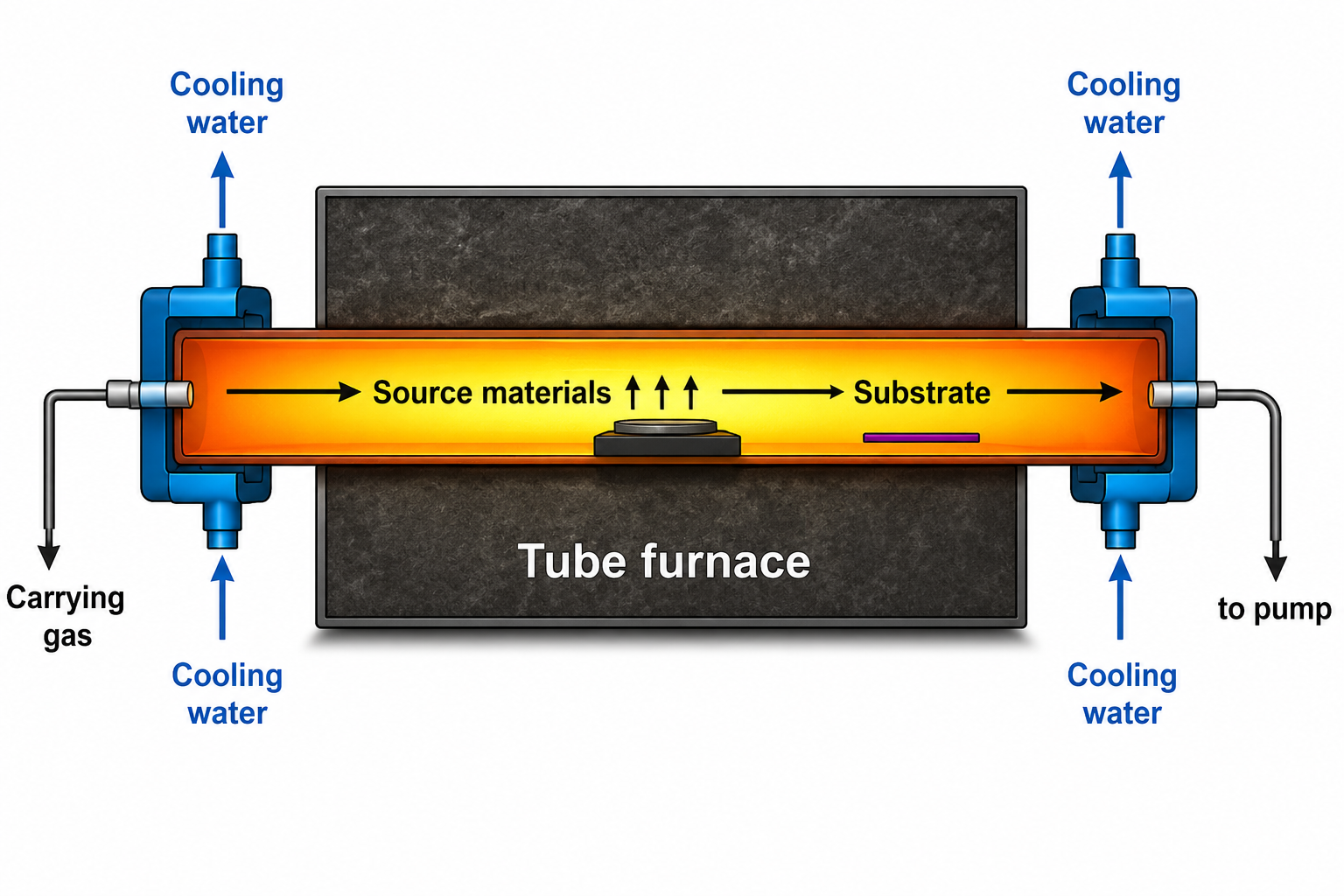

In physical vapour deposition (PVD), the source material is physically converted to vapour — by thermal evaporation (resistive or electron-beam heating) or by momentum transfer from an energetic ion beam (sputtering) — and the vapour condenses on the cooler substrate. The process is purely physical: no chemistry occurs between precursor and substrate. PVD is line-of-sight, meaning the growing film faithfully replicates the source-to-substrate geometry and can leave shadowed regions uncoated — a limitation for high-aspect-ratio trenches, but a useful patterning strategy in other contexts.
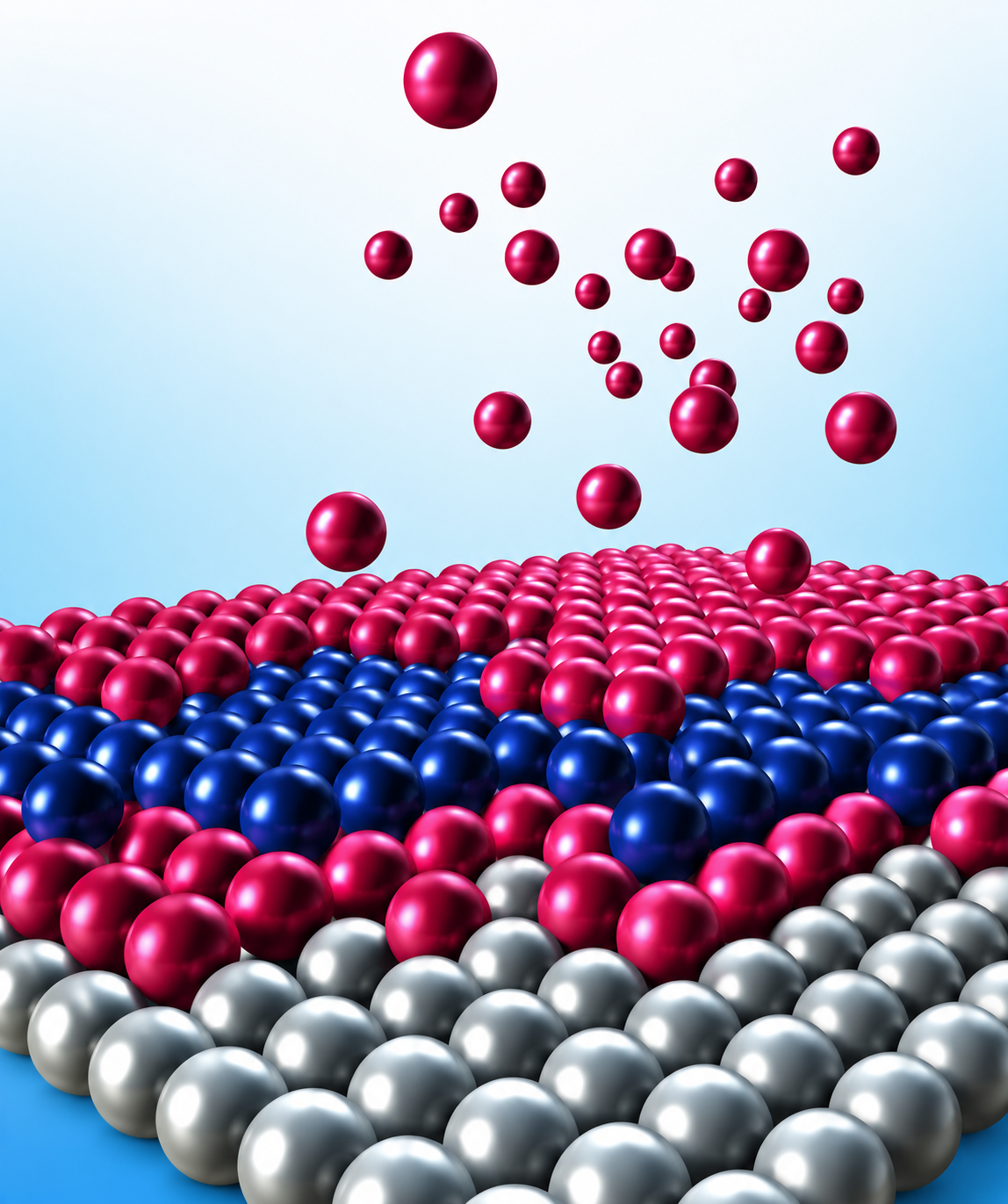
In chemical vapour deposition (CVD), gaseous precursor molecules flow over a heated substrate and undergo heterogeneous chemical reactions at or near the surface, depositing a solid film. Because the precursor gas fills the entire reactor volume, CVD provides excellent step coverage — coating all surfaces uniformly, including the deep walls of high-aspect-ratio features that PVD cannot reach. CVD is used to deposit silicon, SiO₂, Si₃N₄, tungsten, and epitaxial compound semiconductors, as well as graphene and carbon nanotubes. The trade-off is reactor complexity: precursor chemistry, pressure, temperature, and gas flow must all be precisely controlled.
7 Etching — Sculpting Matter by Selective Removal
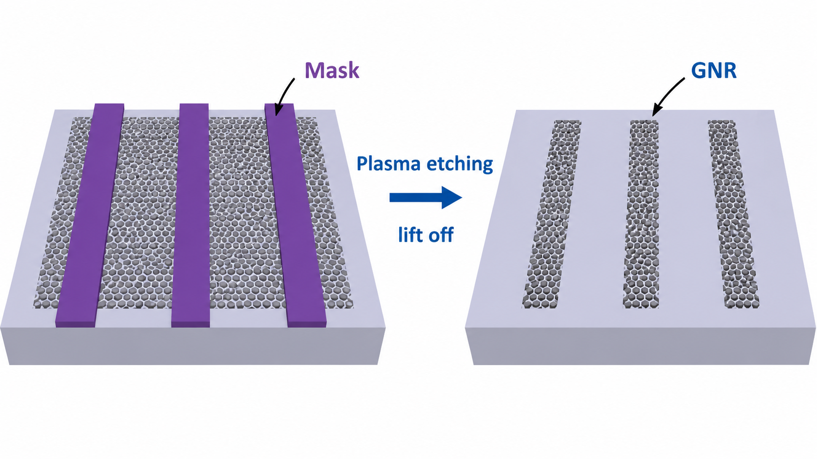
Etching is the complement of deposition: material is selectively removed from regions of a substrate not protected by a mask. It is through repeated cycles of deposition and etching — sometimes dozens of cycles in a single device process flow — that the intricate three-dimensional architectures of modern integrated circuits are constructed. Etching is broadly classified as wet (chemical solution) or dry (plasma-based), and each class has distinct characteristics regarding isotropy, selectivity, and minimum achievable feature size.
Wet chemical etching uses acidic or basic solutions. For silicon, HF/HNO₃ mixtures etch rapidly; for SiO₂, buffered HF (BHF) is highly selective over silicon. In amorphous or polycrystalline materials, wet etching is isotropic — it proceeds equally in all directions from the mask opening, creating a curved undercut profile that limits minimum resolvable feature size. In single-crystal materials, anisotropic wet etching exploits differential dissolution rates between crystallographic planes: KOH selectively attacks the Si{100} planes, leaving atomically smooth {111} sidewalls inclined at 54.7°. This crystallographic anisotropy is the basis of MEMS accelerometer fabrication.
Dry plasma etching — particularly reactive-ion etching (RIE) — overcomes isotropy. In RIE, a radio-frequency plasma generates reactive radicals that chemically attack the substrate, while energetic ions are accelerated perpendicular to the wafer by the plasma sheath electric field. The combination of directional ion bombardment and chemical reactivity produces highly anisotropic etching: near-vertical sidewalls with aspect ratios exceeding 50:1 are achievable with the Bosch process (alternating cycles of etching and polymer passivation). This capability is essential for the through-silicon vias used in 3D chip stacking and the deep trenches of DRAM capacitors.
8 Micromachining & CVD vs. PVD
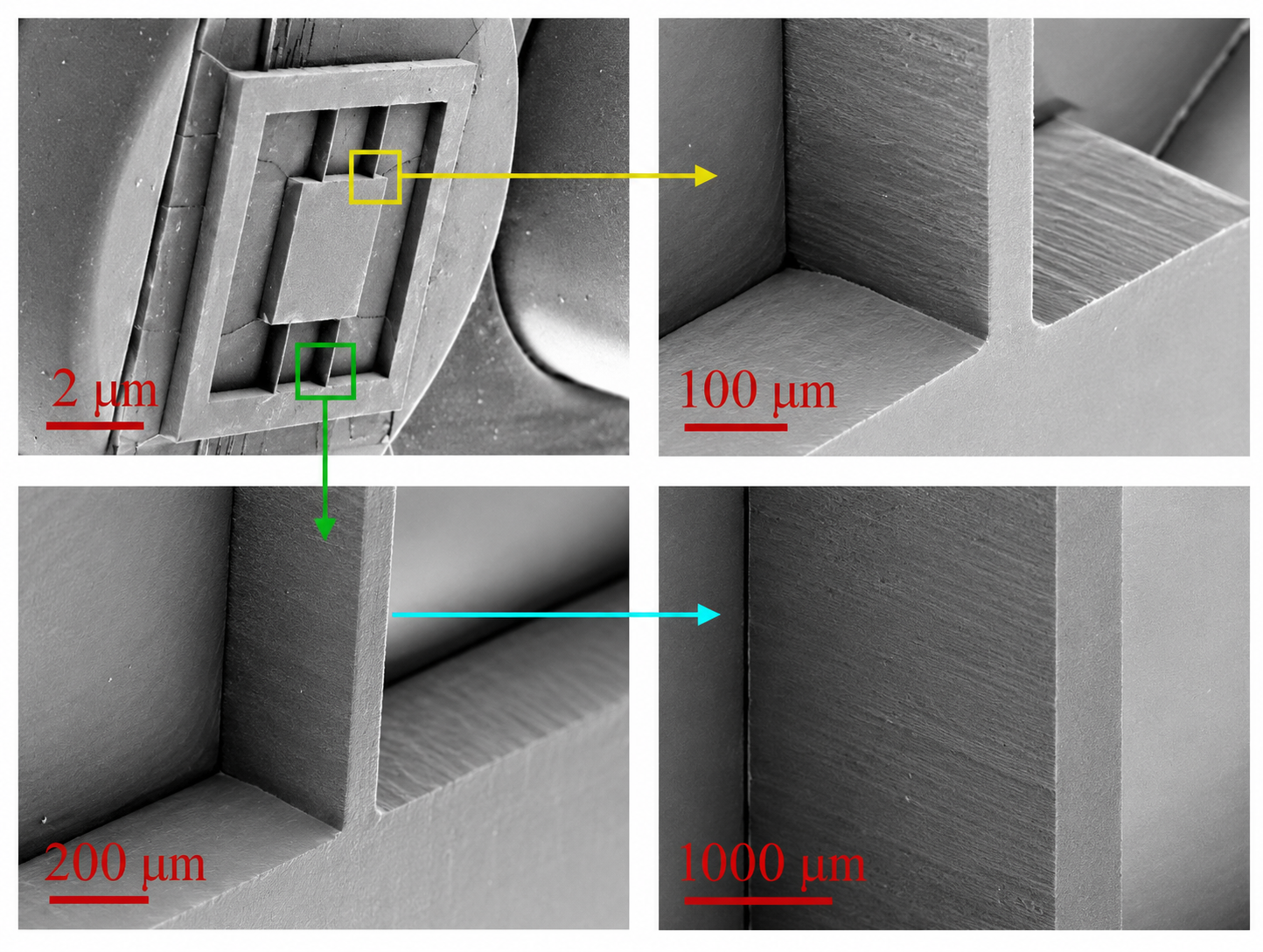
Micromachining extends patterning and etching into the third dimension, creating free-standing mechanical structures from deposited films or from the silicon substrate itself. It is the manufacturing backbone of microelectromechanical systems (MEMS) — the accelerometers, gyroscopes, pressure sensors, and microfluidic devices that pervade modern technology.
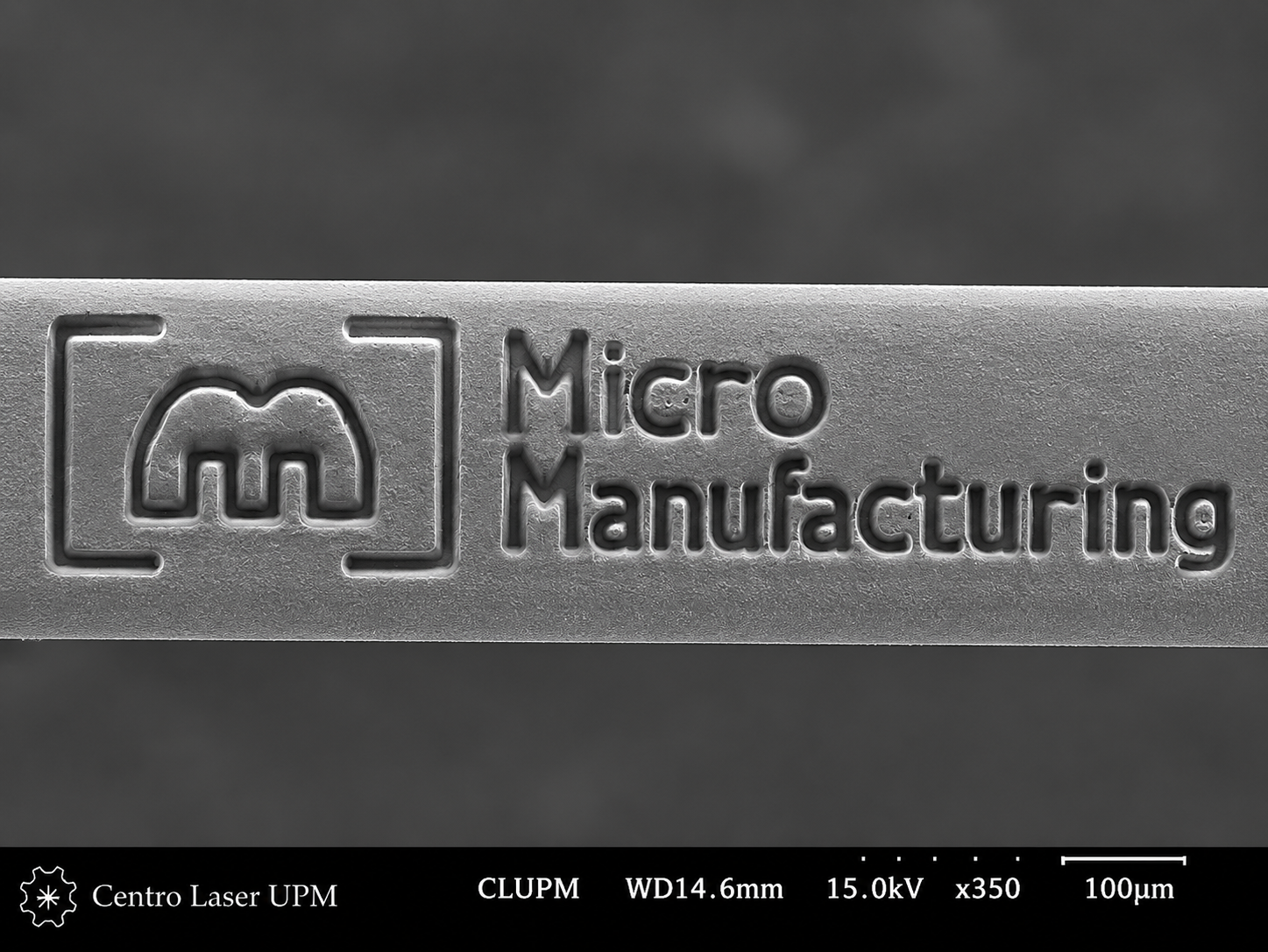
The distinction between CVD and PVD becomes particularly important in understanding how thin films are grown in micromachined device stacks.
9 Self-Assembly — Order from Molecular Forces
Self-assembly is perhaps the most philosophically distinct of all nanofabrication strategies, because it relies on thermodynamic driving forces to organise matter spontaneously into ordered structures — without a human placing each component. It is defined precisely as the spontaneous association of molecules under near-equilibrium conditions into stable, structurally well-defined aggregates. The key word is "spontaneous": the process is driven entirely by minimisation of free energy, not by external mechanical manipulation.
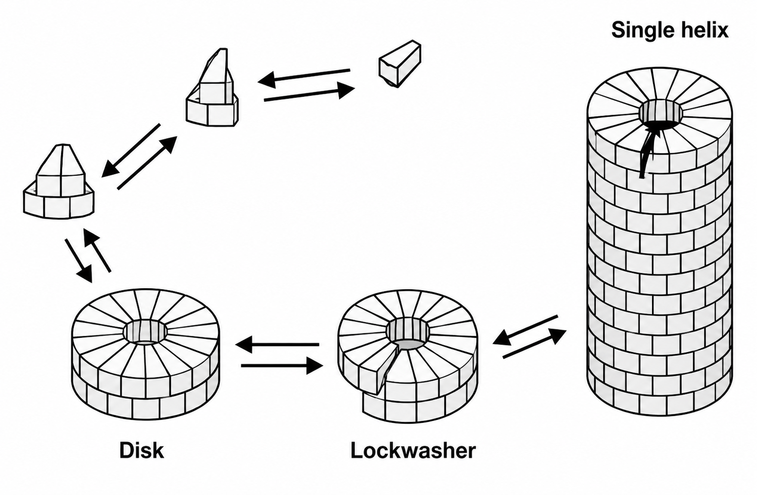
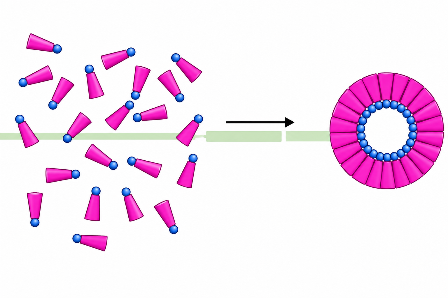
In materials engineering, self-assembly manifests in several practically important forms beyond biological systems. Block copolymers — chains of two chemically distinct polymer segments joined end-to-end — microphase-separate spontaneously into periodic lamellar, cylindrical, or spherical morphologies with domain spacings of 5–50 nm. These patterns can serve as nanolithography templates, effective extending optical lithography resolution into the sub-10 nm regime. Colloidal nanoparticles with engineered surface chemistry self-organise into superlattices. DNA origami uses programmable base-pairing to fold DNA into arbitrary 2-D and 3-D shapes — a technique that has produced drug-delivery nanocapsules, nanoscale robots, and precisely positioned nanoparticle arrays.
10 Classifying Nanomaterials — Dimensionality
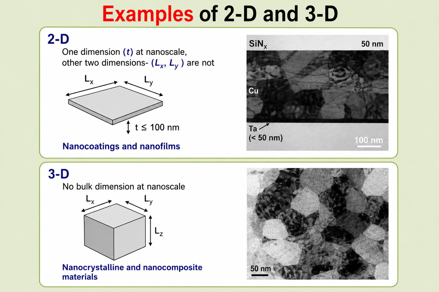
Having surveyed how nanomaterials are made, it is essential to establish a rigorous framework for classifying what is made. The most widely adopted scheme organises nanomaterials according to how many of their physical dimensions fall within the nanoscale range (1–100 nm). This dimensionality classification is not merely taxonomic — it directly predicts the nature and magnitude of quantum confinement effects, which govern electronic, optical, magnetic, and catalytic properties.
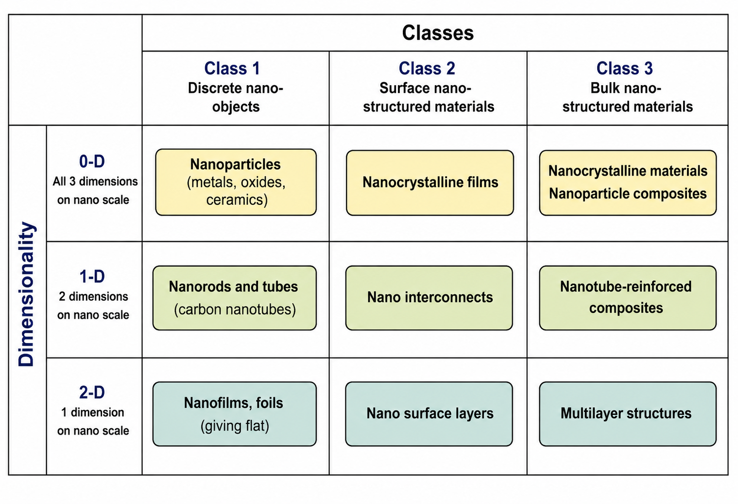
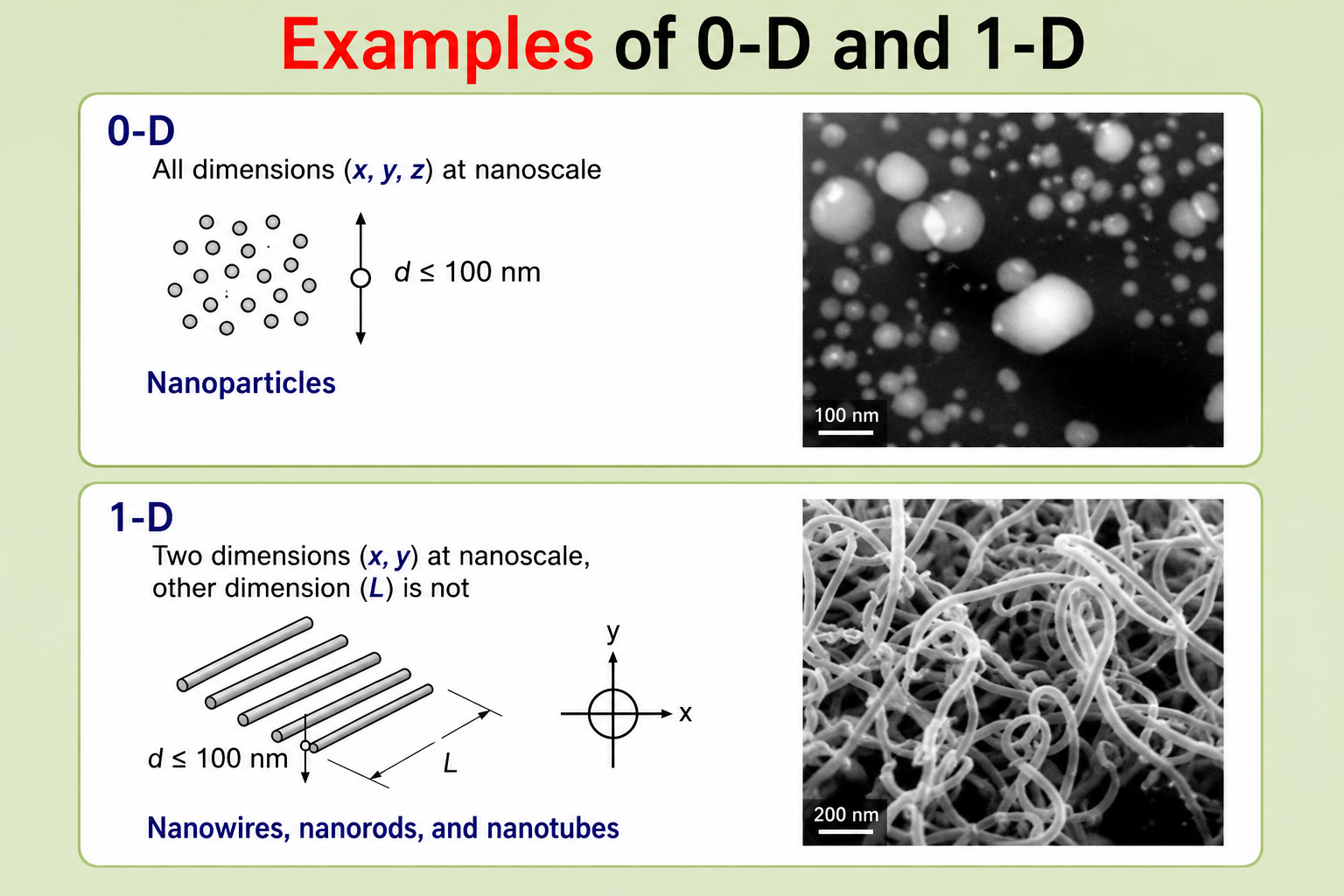
11 Characterising Nanomaterials by Dimensionality
Each class of nanomaterial demands characterisation tools matched to its geometry and the length scale of its defining structural features. Simply knowing that a material is nanocrystalline or that a film is 20 nm thick is insufficient — the spatial resolution of the instrument must be comparable to or better than the feature of interest. The four dimensionality classes each have preferred characterisation approaches.
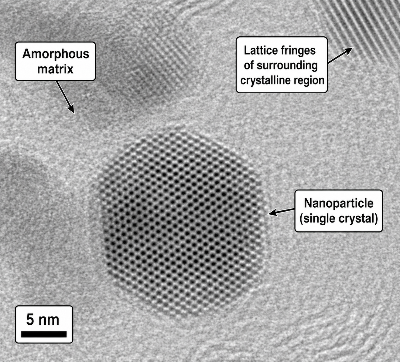
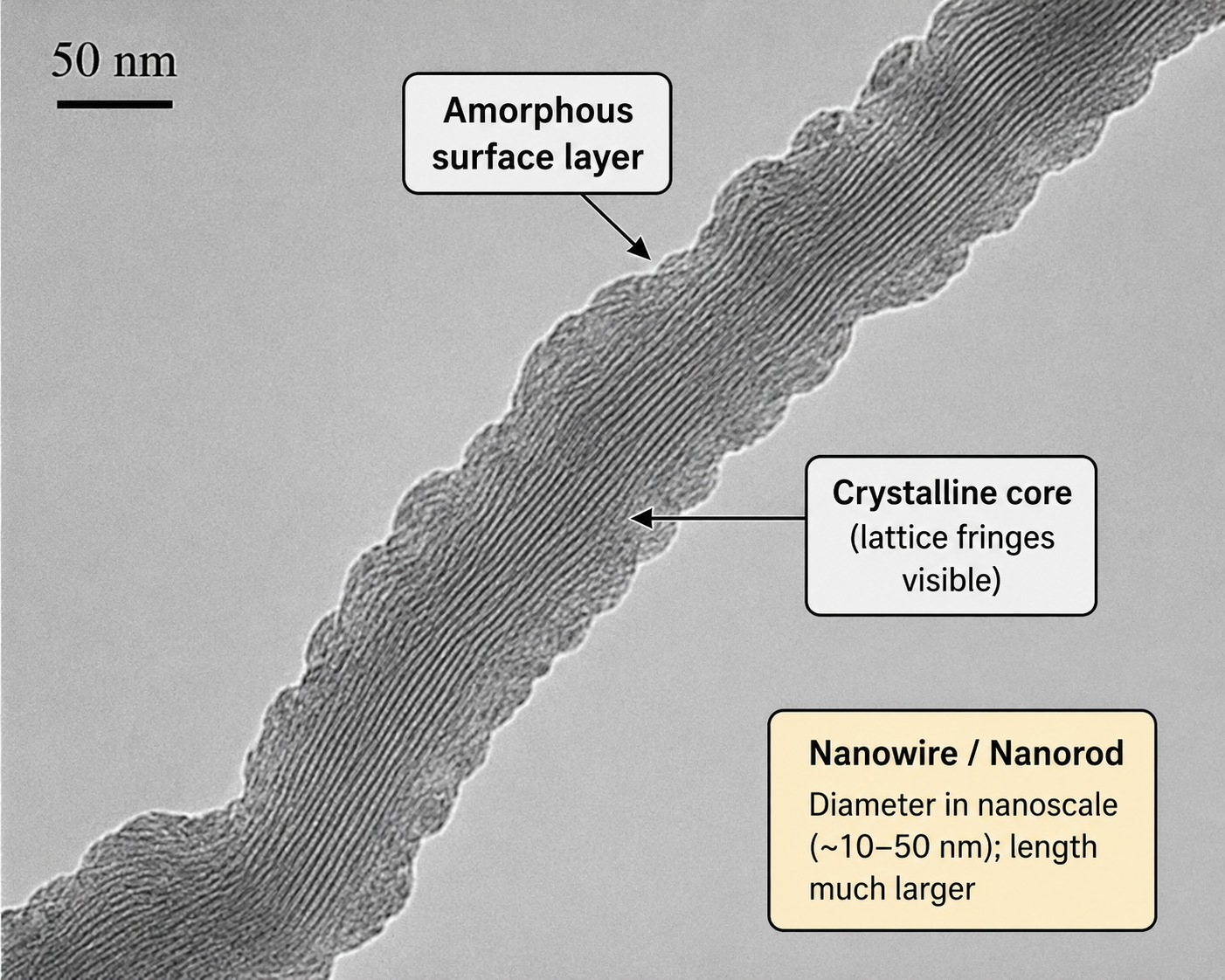
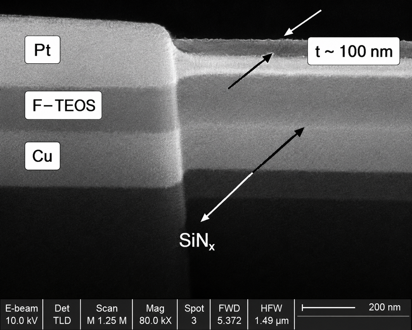
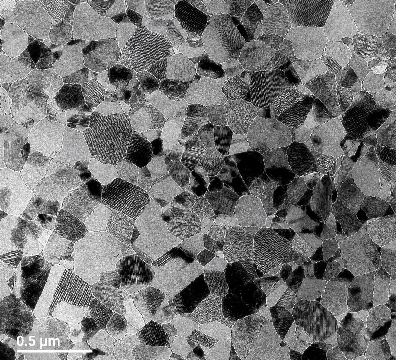
The classification by dimensionality is not just administrative — it directly predicts which quantum mechanical effects will dominate. In a 0-D quantum dot, confinement in all three directions produces discrete, atom-like energy levels and size-tunable photoluminescence. In a 1-D nanotube or nanowire, confinement in two directions quantises transverse electron motion into sub-bands while leaving axial transport essentially free. In a 2-D nanofilm or graphene layer, confinement in one direction produces a two-dimensional electron gas with unique transport properties including the quantum Hall effect. In a 3-D nanocrystalline bulk material, quantum confinement within grains is secondary to the dominant role of grain boundaries in scattering, pinning, and short-circuit diffusion. Understanding which regime a material inhabits is the starting point for all property prediction and materials design at the nanoscale.
✦ References & Further Reading
- Eigler, D. M. & Schweizer, E. K. (1990). Positioning single atoms with a scanning tunnelling microscope. Nature, 344, 524–526.
- Klug, A. (1983). From macromolecules to biological assemblies (Nobel Lecture). Angew. Chem. Int. Ed. Engl., 22, 565–636.
- Madou, M. J. (2011). Fundamentals of Microfabrication and Nanotechnology (3rd ed.). CRC Press.
- Wang, X. & Shi, G. (2015). Graphene: An Introduction to the Fundamentals and Industrial Applications. Wiley-Scrivener.
- Cao, G. (2004). Nanostructures & Nanomaterials: Synthesis, Properties & Applications. Imperial College Press.
- Murty, B. S., Shankar, P., Raj, B., Rath, B. B. & Murday, J. (2013). Textbook of Nanoscience and Nanotechnology. Universities Press–IIM.
Nanomaterial Dimensionality & Nanostructure Classification
How reducing dimensions to the nanoscale changes the rules: quantum confinement, density of states, and the taxonomy of zero-, one-, and two-dimensional nanostructures.
Contents
- Why Grain Size Matters: Property Changes in Nanocrystalline Nickel
- Electron Delocalization and Quantum Confinement
- Particle-in-a-Box: Quantised Energy Levels
- Visualising Dimensionality: The Nanostructure Taxonomy
- Aspects of 2-D Nanostructures: Films and Coatings
- Three-Dimensional Nanocrystalline Materials in Bulk Form
- Summary of Crystalline Nanostructure Types
- Nanocomposites: Matrix-Reinforced and Layered Architectures
- From Basic Geometry to Large-Scale Nanocomposite Forms
- Patterned 2-D Nanomaterials: Channels and Holes at the Nanoscale
- Functional Nanostructures: Copper Interconnects
- General Characteristics by Nanomaterial Class and Dimensionality
- Surface-to-Volume Ratio: The Geometric Basis of Nanoscale Advantage
- Quantitative Example: Surface Area, Volume, and Radius in Quantum Dots
- References & Further Reading
1 Why Grain Size Matters: Property Changes in Nanocrystalline Nickel
One of the most compelling early demonstrations of the transformative power of nanoscale grain refinement came from systematic studies on nanocrystalline nickel. When the grain size of nickel is reduced to approximately 10 nm — a regime where grain boundaries constitute a significant volume fraction of the material — the resulting property changes are not merely incremental. They are dramatic and, in some cases, counterintuitive.
Mechanically, a fivefold increase in hardness is observed. Tensile strength increases by a factor of three to ten, and wear resistance rises by a staggering 170 times compared to conventional coarse-grained nickel. The frictional coefficient is halved, which has profound implications for tribological applications. These improvements are well explained by classical Hall–Petch strengthening: as grain size d decreases, the yield stress scales as d−½ because grain boundaries act as barriers to dislocation motion, forcing dislocations to pile up before they can propagate.
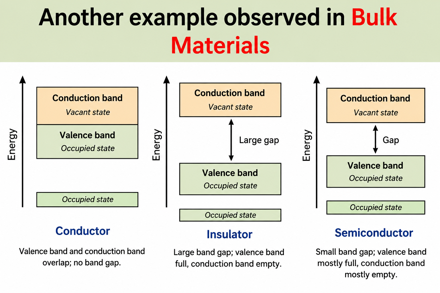
Fig. 3.1 Band structure of conductors, insulators and semiconductors, showing the relative positions of the valence band and conduction band and the role of the band gap in determining electrical character. This diagram motivates why quantum confinement — which widens the effective gap in nanomaterials — can tune a semiconductor's optical and electronic properties.
Corrosion resistance, however, tells a different story: it decreases in nanocrystalline nickel. This is because the vast grain boundary network provides high-diffusivity pathways for corrosive species, and the elevated internal energy of grain boundary atoms lowers the thermodynamic barrier to oxidation and dissolution. Similarly, saturation magnetisation decreases by roughly 5%, electrical resistivity increases (due to enhanced grain-boundary scattering of electrons), and hydrogen diffusion increases — all consequences of the same boundary-dominated microstructure that confers such extraordinary mechanical strength.
The underlying reason for all these changes is the same: as grain size decreases, the fraction of atoms residing at or near grain boundaries rises sharply. Atoms at boundaries are in a disordered, higher-energy environment with modified interatomic distances and coordination numbers. Since virtually every mode of material failure or degradation involves the initiation and propagation of defects, and since grain boundaries are the dominant defect in nanocrystalline materials, the entire property profile shifts to reflect boundary-governed behaviour rather than the lattice-governed behaviour seen in bulk polycrystals.
2 Electron Delocalization and Quantum Confinement
A fundamentally different mechanism operates at even smaller length scales — one rooted not in defect density but in quantum mechanics. In conventional bulk metals and semiconductors, conduction electrons are delocalized: their wavefunctions extend coherently throughout the crystal lattice, giving rise to the continuous energy bands described by band theory. This delocalization underpins the concepts of electrical conductivity, optical absorption, and thermal transport that engineers rely upon every day.
When a material's dimensions shrink to the nanoscale — particularly below the de Broglie wavelength of an electron, typically a few to tens of nanometres — this delocalization is constrained. The dimensionality of confinement determines how severely electron motion is restricted:
- 0-D (quantum dot): Electron confined in all three spatial dimensions — no free delocalization in any direction.
- 1-D (quantum wire): Electron delocalized only along the wire length; confined in the two transverse directions.
- 2-D (quantum well): Electron delocalized in the plane; confined only through the thickness dimension.
- 3-D (bulk material): Electrons freely delocalized in all three dimensions — classical band-theory applies.
This classification is not merely taxonomic. It has direct physical consequences for the density of electronic states and, through that, for every observable property that depends on electronic structure: optical absorption wavelength, fluorescence emission, electrical conductivity, thermoelectric performance, and catalytic reactivity.
3 Particle-in-a-Box: Quantised Energy Levels
The energetic consequences of quantum confinement are most clearly captured by the quantum-mechanical model of a particle confined within an infinite potential well — the "particle in a box." In this model, an electron occupying a perfectly confining nanostructure (a deep potential well with perfectly hard walls) cannot escape and cannot occupy arbitrary energies. Instead, only discrete energy levels are permitted, their spacing determined by the size of the box.
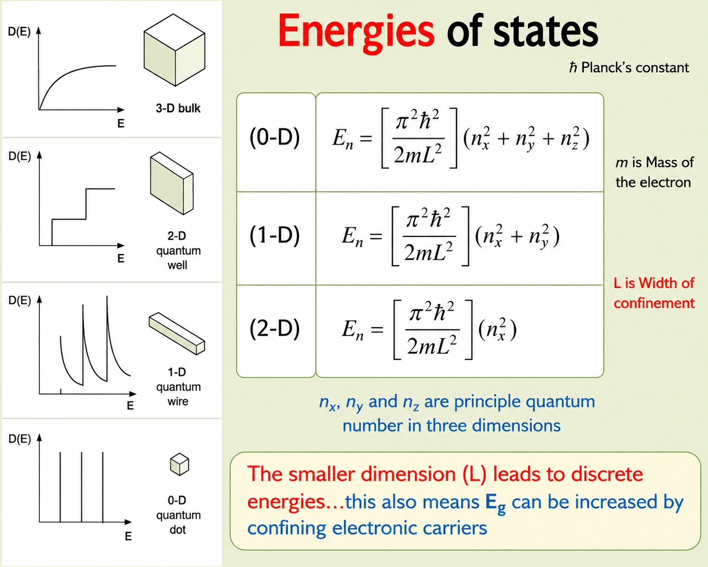
Fig. 3.2 Density of states D(E) as a function of energy E for materials of different dimensionality, together with the particle-in-a-box energy equations governing each case. The 3-D bulk shows a smooth parabolic DOS; the 2-D quantum well shows staircase-like steps; the 1-D quantum wire shows sharp inverse-square-root peaks; the 0-D quantum dot shows discrete delta-function-like states — a direct consequence of progressive confinement.
The allowed energy levels in each dimensionality are given by the particle-in-a-box formulation, where ℏ is the reduced Planck constant, m is the electron mass, L is the confinement dimension, and nx, ny, nz are the principal quantum numbers in the three spatial dimensions:
- 0-D (quantum dot): En = (π²ℏ²/2mL²)(nx² + ny² + nz²) — confined in all three dimensions
- 1-D (quantum wire): En = (π²ℏ²/2mL²)(nx² + ny²) — free along z, confined in x and y
- 2-D (quantum well): En = (π²ℏ²/2mL²)(nx²) — free in y and z, confined only in x
The critical insight is that as the confinement dimension L decreases, the energy spacing between levels increases as 1/L². This means that by making a nanostructure smaller, one can physically tune the energy gap Eg — the separation between the highest occupied and lowest unoccupied states. In semiconductor quantum dots, for instance, this is precisely what causes the well-known size-dependent fluorescence: smaller dots emit higher-energy (shorter wavelength, bluer) light; larger dots emit lower-energy (longer wavelength, redder) light. Engineering L is, in effect, engineering the optical spectrum — something impossible in bulk materials.
The ability to control the density of electronic states through confinement opens doors to applications in infrared detectors, high-temperature superconductors, biological imaging tags, optical memories, and photonic structures. Each of these exploits the fact that nanoconfinement converts the continuous energy bands of bulk into a structured, tunable spectrum.
4 Visualising Dimensionality: The Nanostructure Taxonomy
Having established the physical origins of dimensionality-dependent behaviour, it is useful to develop a concrete visual and conceptual taxonomy of nanostructure types. The classification proceeds from the most highly confined (0-D) to the least confined (3-D), with each class exhibiting its own characteristic geometry, synthesis challenges, and application profile.
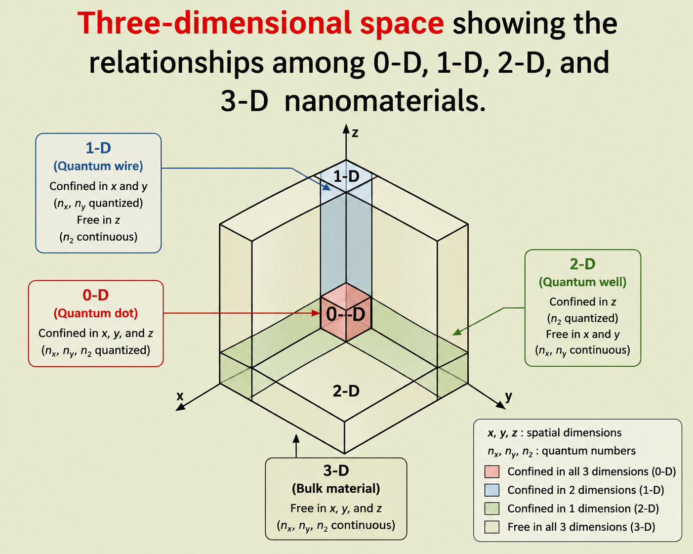
Fig. 3.3 Isometric three-dimensional space illustrating the spatial relationships among 0-D, 1-D, 2-D, and 3-D nanomaterials. The 0-D point occupies the corner (all dimensions nanoscale); the 1-D wire extends along one axis; the 2-D surface fills a face; the 3-D bulk fills the entire volume with internal nanoscale grain structure.
5 Aspects of 2-D Nanostructures: Films and Coatings
Two-dimensional nanomaterials are characterised by nanoscale thickness (t ≤ 100 nm) in one direction, with macroscopic or microscopic lateral dimensions in the other two. The internal crystalline structure — nanocrystalline or microcrystalline — provides a second axis of classification, giving rise to a rich matrix of two-dimensional nanostructure types.
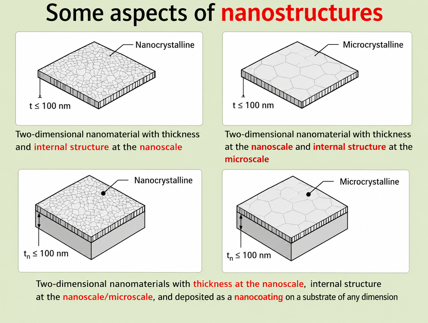
Fig. 3.4 Aspects of 2-D nanostructures. Top row: freestanding nanocrystalline (left) and microcrystalline (right) thin films, both with thickness t ≤ 100 nm. Bottom row: nanocrystalline and microcrystalline films deposited as nanocoatings on a substrate of arbitrary dimension, with the nanoscale confined to the coating thickness tn ≤ 100 nm and internal structure ranging from nanoscale to microscale.
A nanocrystalline film with thickness at the nanoscale and internal grain structure also at the nanoscale represents the most completely nanoscale two-dimensional material. A microcrystalline film with nanoscale thickness but microscale internal grain structure is still considered a 2-D nanomaterial by virtue of its dimensional constraint in the thickness direction, even though the grain boundaries themselves are widely spaced. The third category — a nanocoating deposited on a substrate of any size — is technologically the most prevalent: hard coatings for cutting tools, anti-reflection coatings for optics, diffusion barriers in microelectronics, and corrosion-resistant layers all belong here.
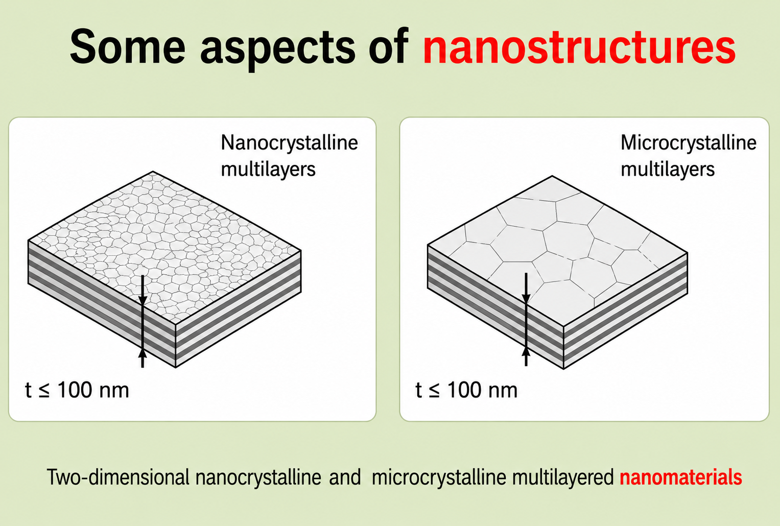
Fig. 3.5 Two-dimensional nanocrystalline (left) and microcrystalline (right) multilayered nanomaterials. Each individual layer has thickness t ≤ 100 nm. Multilayer stacks of this kind are the basis of giant magnetoresistance (GMR) sensors, anti-reflection coatings, and thermal barrier systems in turbine blades.
6 Three-Dimensional Nanocrystalline Materials in Bulk Form
Three-dimensional nanocrystalline nanomaterials represent the case where all three macroscopic dimensions of the object are at the micro- or macroscale, but the internal microstructure — specifically the grain size d — is confined to the nanoscale. These are, in everyday terms, bulk objects: rods, plates, ingots, or forgings that can be held in the hand, yet whose grain structure is invisible to all but the most powerful microscopes.
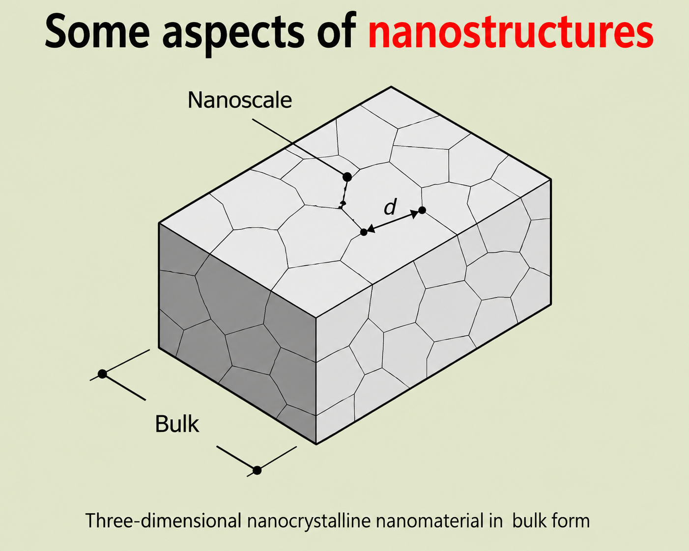
Fig. 3.6 Three-dimensional nanocrystalline nanomaterial in bulk form. The macroscopic object has conventional bulk dimensions, but the internal polycrystalline grain size d is at the nanoscale. This architecture underlies nanocrystalline metals produced by severe plastic deformation, inert-gas condensation, or electrodeposition — delivering extraordinary combinations of strength and hardness.
The manufacture of bulk nanocrystalline materials is technically demanding precisely because the nanoscale grain structure is thermodynamically metastable. Without grain boundary stabilisers — solute additions that reduce grain boundary energy or mobility — the nanostructure will coarsen under moderate heating as the system minimises its total grain boundary area. Techniques such as severe plastic deformation (ECAP, high-pressure torsion), inert-gas condensation followed by compaction, and electrodeposition are the principal routes to bulk nanocrystalline metals and alloys.
7 Summary of Crystalline Nanostructure Types
A comprehensive taxonomy of two-dimensional and three-dimensional crystalline nanostructures organises the landscape of nanomaterials in a way that is directly useful for engineering design. The central parameter is the relationship between the nanoscale dimension and the substrate, coating, or internal grain structure.
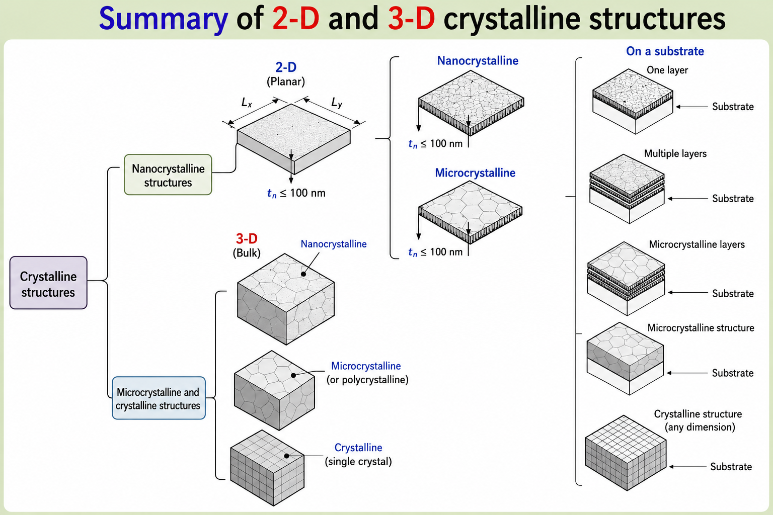
Fig. 3.7 Summary classification of two-dimensional and three-dimensional crystalline nanostructures. Nanocrystalline structures branch into freestanding nanocrystalline films (deposited as single or multiple layers on substrates) and microcrystalline structures with nanoscale coatings. The tree terminates at fully crystalline bulk structures of any dimension, which represent the transition back to macroscale materials engineering.
8 Nanocomposites: Matrix-Reinforced and Layered Architectures
When a nanoscale reinforcement phase is embedded within or deposited upon a matrix material, the result is a nanocomposite. Nanocomposites represent one of the most technologically significant branches of nanomaterials engineering because they allow property combinations not achievable in monolithic systems: the matrix provides toughness and processability, while the nanoscale reinforcement delivers hardness, stiffness, conductivity, or other specific properties.
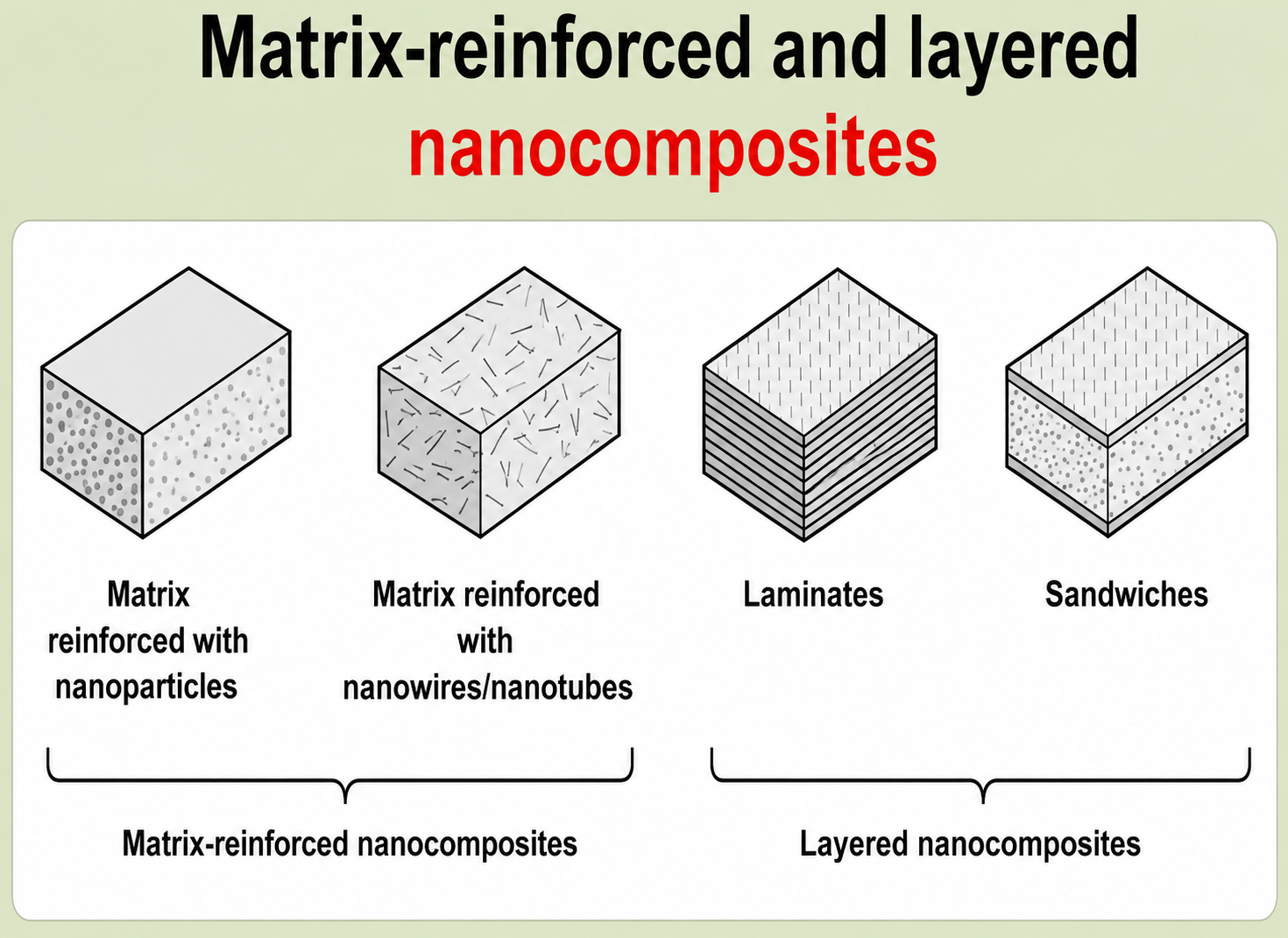
Fig. 3.8 Matrix-reinforced and layered nanocomposite architectures. Left pair (matrix-reinforced nanocomposites): a matrix containing dispersed nanoparticles, and a matrix reinforced with nanowires or nanotubes. Right pair (layered nanocomposites): alternating laminates of two distinct materials, and sandwich architectures with thick outer skins and a nanoscale-structured core.
Matrix-reinforced nanocomposites using carbon nanotubes achieve exceptional combinations of stiffness and electrical conductivity. Particulate-reinforced systems using ceramic nanoparticles in a metal matrix are the basis of next-generation cutting tools and wear-resistant coatings. Layered nanocomposites — laminates and sandwiches — exploit the stiffness anisotropy and interface density of thin film stacks to provide exceptional in-plane load-bearing capacity with low weight.
9 From Basic Geometry to Large-Scale Nanocomposite Forms
One of the most practically important aspects of nanomaterial science is understanding how the basic nanoscale geometry — point (0-D), line (1-D), or surface (2-D) — translates into large-scale usable forms. In engineering applications, nanomaterials are rarely used as isolated particles or wires; they are incorporated into thick films, bulk composites, or coated substrates whose macroscopic dimensions are at the micro- or macroscale, even as the internal structure remains nanoscale.
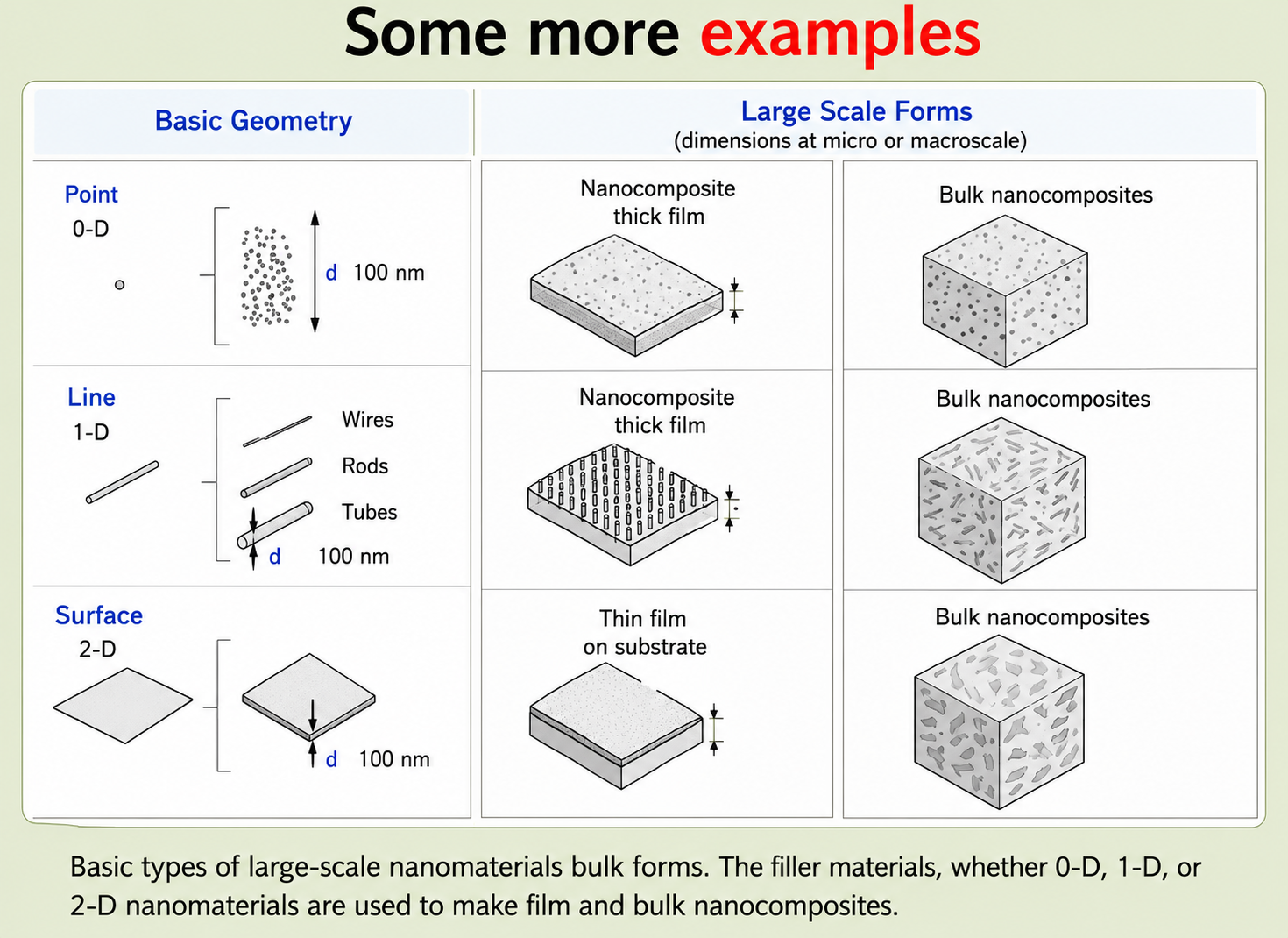
Fig. 3.9 Relationship between basic nanoscale geometry and large-scale engineering forms. Point-geometry (0-D) nanoparticles can be consolidated into nanocomposite thick films or bulk nanoparticle composites. Line-geometry (1-D) nanowires, rods, and tubes form the basis of nanocomposite thick films and fibre-reinforced bulk composites. Surface-geometry (2-D) thin films are deposited directly on substrates or assembled into bulk layered composites. In each case, the filler material geometry defines the final composite architecture.
10 Patterned 2-D Nanomaterials: Channels and Holes at the Nanoscale
A particularly sophisticated sub-class of two-dimensional nanomaterials carries not just nanoscale thickness but also nanoscale patterned features — channels, holes, ridges, and trenches etched or deposited into the film plane. These patterned structures are the backbone of microfluidic devices, lab-on-chip systems, photonic crystal slabs, and nanoimprint lithography templates.
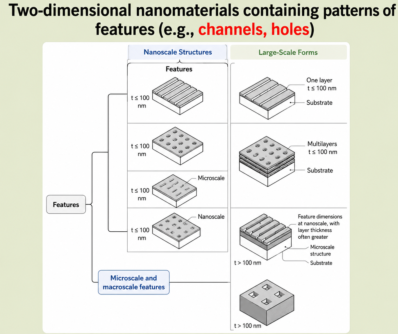
Fig. 3.10 Classification of two-dimensional nanomaterials containing patterns of features such as channels and holes. Nanoscale features (t ≤ 100 nm) embedded within films of nanoscale thickness give rise to purely nanoscale patterned structures. When feature dimensions are at the nanoscale but the surrounding layer thickness exceeds 100 nm, the structure straddles the nano–microscale boundary. Large-scale forms include single-layer substrates, multilayer stacks, and microscale structures with embedded nanoscale features.
11 Functional Nanostructures: Copper Interconnects
To ground the taxonomy in a real engineering application, consider nanocopper interconnects — the conducting lines that wire together transistors on a modern integrated circuit. As transistor dimensions have scaled below 100 nm, the width of the copper lines connecting them has followed. These nanoscale conductors are produced not by casting or rolling but by electrodeposition: copper is electrochemically deposited into nanoscale channels previously patterned into a dielectric material (typically low-k SiO₂ or SiCOH) using photolithography and reactive-ion etching.
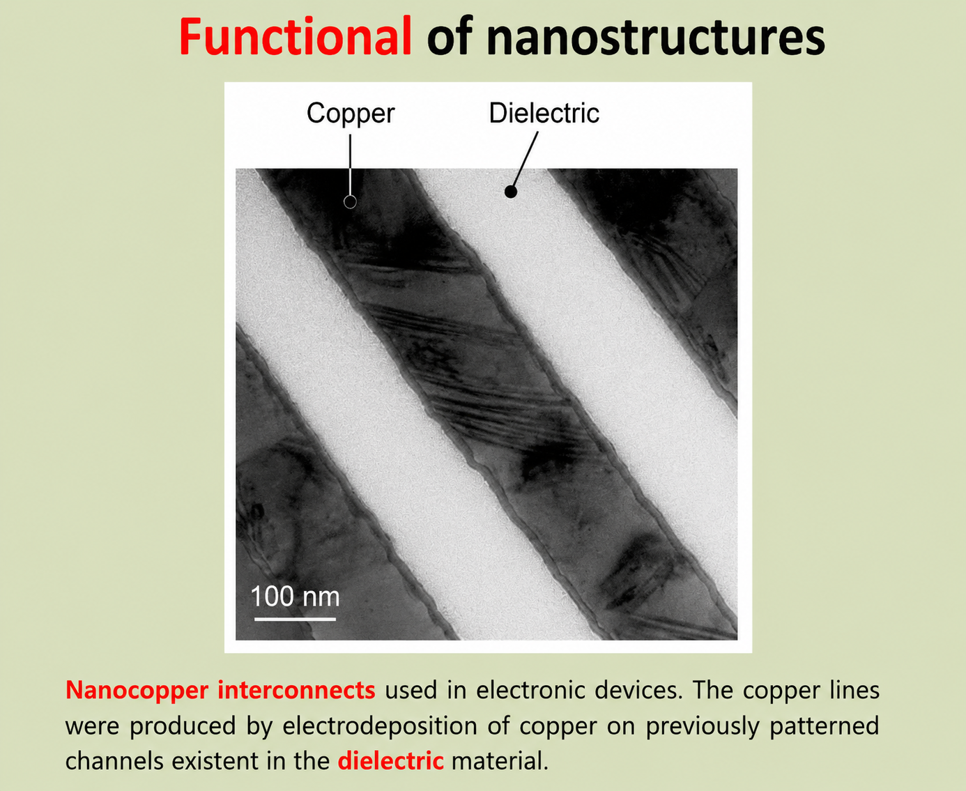
Fig. 3.11 Transmission electron microscopy (TEM) image of nanocopper interconnects embedded in a dielectric matrix. The bright regions are copper lines produced by electrodeposition into pre-patterned channels. The 100 nm scale bar illustrates the truly nanoscale dimensions of these conductors. At this scale, grain boundary scattering and surface scattering significantly increase electrical resistivity relative to bulk copper, a key challenge in advanced semiconductor nodes.
At these dimensions, the classical Drude model of electrical conduction breaks down. The mean free path of electrons in bulk copper (~40 nm at room temperature) is comparable to or larger than the interconnect width, so electrons scatter preferentially from grain boundaries and the copper line surfaces rather than from phonons. This size-induced resistivity increase is one of the most pressing challenges in semiconductor interconnect scaling, driving research into alternative conductor materials such as cobalt, ruthenium, and molybdenum for sub-10 nm nodes.
12 General Characteristics by Nanomaterial Class and Dimensionality
Bringing the taxonomy together, it is possible to construct a comprehensive matrix that crosses the dimensionality axis (0-D, 1-D, 2-D) with the class axis (discrete nano-objects, surface nano-featured materials, bulk nanostructured materials). This provides a rapid reference framework for identifying where a given material or application fits within the broader nanomaterials landscape.
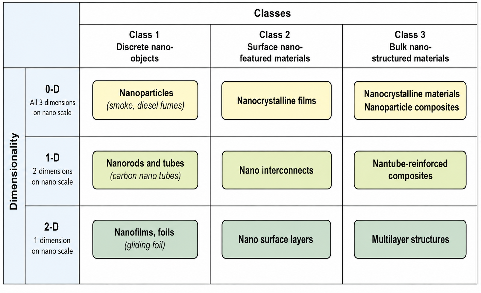
Fig. 3.12 General characteristics of nanomaterial classes and dimensionality. Class 1 (discrete nano-objects): 0-D nanoparticles and smoke; 1-D nanorods and carbon nanotubes; 2-D nanofilms and gilding foils. Class 2 (surface nano-featured): 0-D nanocrystalline films; 1-D nano interconnects; 2-D nano surface layers. Class 3 (bulk nanostructured): 0-D nanocrystalline materials and nanoparticle composites; 1-D nanotube-reinforced composites; 2-D multilayer structures.
13 Surface-to-Volume Ratio: The Geometric Basis of Nanoscale Advantage
The most universal and quantitative argument for why nanoscale materials behave differently from their bulk counterparts is the surface-to-volume ratio. As a material is subdivided into smaller and smaller pieces — at constant total mass — the total surface area increases while the total volume remains constant. The surface-to-volume ratio therefore increases with decreasing size, and at the nanoscale, this increase becomes enormous.
For a sphere of radius r, the surface area is 4πr² and the volume is (4/3)πr³, giving a surface-to-volume ratio of 3/r. For a cube of side L, the ratio is 6/L. For a cylinder of radius r and length h much greater than r, the ratio is approximately 2/r. In each case, the ratio scales as the inverse of the characteristic dimension — meaning that halving the particle size doubles the surface-to-volume ratio.
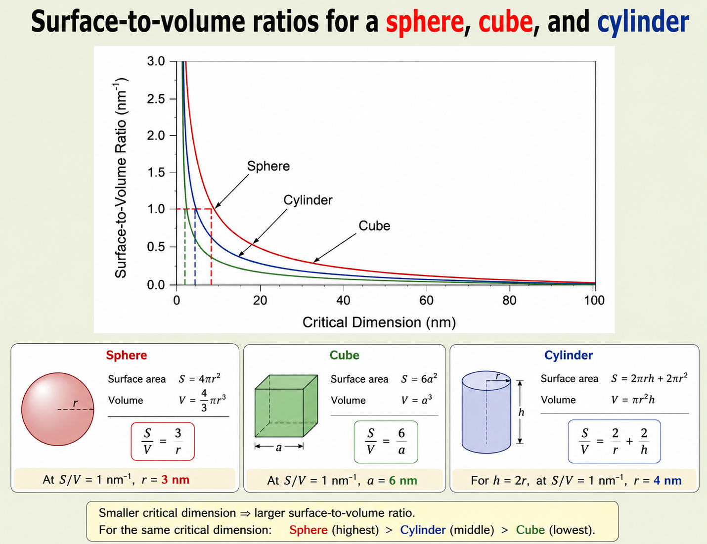
Fig. 3.13 Surface-to-volume ratio as a function of critical dimension (nm) for a sphere, cylinder, and cube. All three geometries show a steep, hyperbolic increase in S/V ratio as the dimension decreases below 20 nm, with the sphere consistently exhibiting the highest ratio at all sizes. At 1 nm, S/V values exceed 2–3 nm⁻¹, corresponding to essentially all atoms being surface atoms. This graph quantifies why nanomaterials are dominated by surface effects.
14 Quantitative Example: Surface Area, Volume, and Radius in Quantum Dots
To make the surface-to-volume relationship concrete, consider a series of spherical quantum dots of decreasing radius. For a dot with radius r = 8 nm, the surface area is 806 nm² and the volume is 2145 nm³, giving S/V = 0.375 nm⁻¹. For r = 6 nm, the surface area falls to 454 nm² and the volume to 905 nm³, giving S/V = 0.501 nm⁻¹. For r = 2 nm, surface area = 50 nm², volume = 34 nm³, and S/V = 1.470 nm⁻¹.
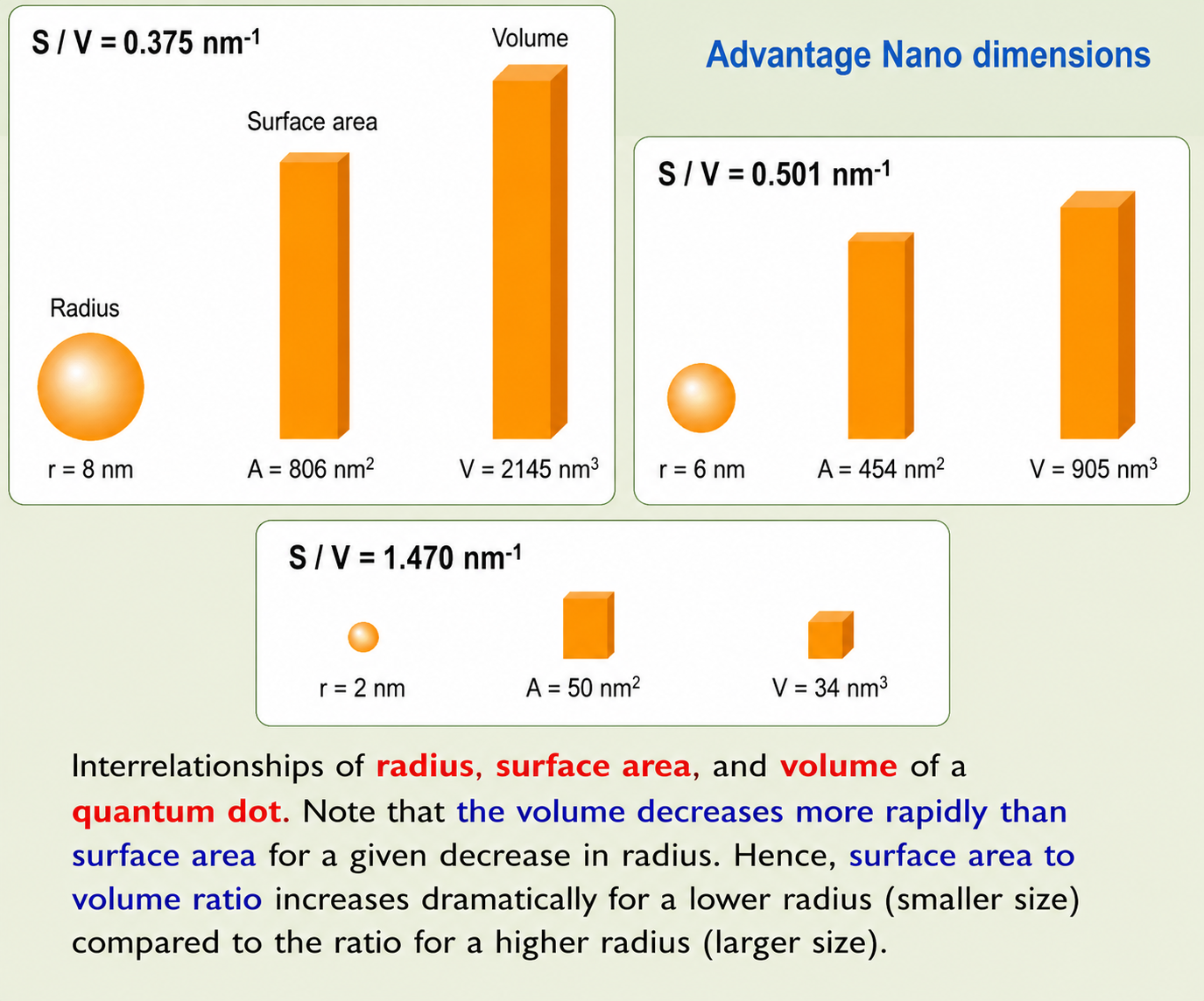
Fig. 3.14 Interrelationships of radius, surface area, and volume for quantum dots at three sizes (r = 8 nm, 6 nm, 2 nm). The orange bar charts illustrate that volume decreases more rapidly than surface area for a given decrease in radius — a direct consequence of the respective cubic and quadratic scaling. The surface-to-volume ratio therefore increases dramatically at lower radii, quantitatively confirming that nanoscale materials are fundamentally surface-dominated.
The key observation — that volume shrinks as r³ while surface area shrinks only as r² — means that the surface fraction of atoms grows without bound as size decreases. At a radius of ~1 nm (roughly 4 atomic diameters in a metal), essentially every atom in the particle is a surface atom. This is the physical basis of the extraordinary catalytic activity of metal nanoparticles: every atom participates in surface chemistry, eliminating the wasted "inactive" bulk atoms of conventional catalysts and dramatically increasing catalytic efficiency per unit mass.
Consider a 1 cm³ cube of iron (atomic diameter of Fe ≈ 0.25 nm). The fraction of surface atoms is negligibly small — well below 0.001%. Now subdivide this cube into smaller cubes with edges of 10 nm: the percentage of surface atoms increases dramatically. At 1 nm³ cube size, every atom in the cube is a surface atom. This thought experiment, calculable from the atomic diameter and cube geometry, powerfully illustrates why nanoscale materials cannot be treated as bulk materials with modified surface areas — they are fundamentally surface-dominated objects.
Key Takeaways
- Reducing grain size to the nanoscale dramatically alters mechanical, electrical, magnetic, and transport properties because grain boundary atoms dominate behaviour.
- Quantum confinement restricts electron delocalization in 0-D, 1-D, and 2-D nanostructures, converting continuous energy bands into discrete or structured density-of-states profiles.
- The particle-in-a-box model shows that energy level spacing scales as 1/L² — smaller confinement dimension means larger energy gaps, enabling tunable optical and electronic properties.
- A systematic taxonomy organises nanomaterials by dimensionality (0-D to 3-D) and class (discrete objects, surface-featured, bulk nanostructured), covering films, composites, patterned structures, and functional nanodevices.
- The surface-to-volume ratio scales as the inverse of the characteristic dimension, making nanomaterials intrinsically surface-dominated and explaining their extraordinary catalytic, optical, and reactive properties.
✦ References & Further Reading
- Murty, B. S., Shankar, P., Raj, B., Rath, B. B. & Murday, J. (2013). Textbook of Nanoscience and Nanotechnology. Universities Press–IIM.
- Cao, G. (2004). Nanostructures & Nanomaterials: Synthesis, Properties & Applications. Imperial College Press.
- Gleiter, H. (2000). Nanostructured materials: basic concepts and microstructure. Acta Materialia, 48(1), 1–29.
- Alivisatos, A. P. (1996). Semiconductor clusters, nanocrystals, and quantum dots. Science, 271(5251), 933–937.
- Siegel, R. W. (1993). Synthesis and properties of nanophase materials. Materials Science and Engineering A, 168(2), 189–197.
- Wolf, E. L. (2015). Nanophysics and Nanotechnology (3rd ed.). Wiley-VCH.
Surface Energy & Nanoscale Phenomena
Surface atoms, the Lycurgus Cup, surface plasmon resonance, Benjamin Franklin's monolayer, and the thermodynamic basis of surface energy in low-index crystal faces.
Contents
- Surface Atoms in Nanoparticles: The Palladium Case
- Surface Energy Increases Catastrophically with Subdivision
- Nanotechnology Is Not a New Phenomenon: The Lycurgus Cup
- Nanomaterials in Art: The Lycurgus Myth and Colloidal Gold
- Surface Plasmon Resonance: The Physical Mechanism
- Benjamin Franklin's Monolayer: An Unwitting Nanoscience Experiment
- Franklin's Experiment as the Basis for Thin Film Technologies
- Surface Energy: Definition and Physical Origin
- Surface Relaxation and Its Effect on Surface Energy
- Surface Energy of Low-Index Crystal Faces
- References & Further Reading
1 Surface Atoms in Nanoparticles: The Palladium Case
The central quantitative argument for why nanoscale materials behave so differently from their bulk counterparts is the dramatic increase in the fraction of atoms residing at the surface. In a bulk crystal, the overwhelming majority of atoms are interior atoms — fully coordinated, surrounded on all sides by neighbours, and largely insulated from the external environment. Surface atoms, by contrast, have broken or unsatisfied bonds, higher energy states, and direct exposure to gases, liquids, and other reactive species. In a macroscopic material, this surface fraction is negligibly small. At the nanoscale, it becomes the dominant characteristic of the material.
Palladium nanoparticles provide one of the most cited quantitative illustrations of this phenomenon. Experimental measurements and theoretical calculations together show that the percentage of surface atoms changes dramatically with cluster diameter. At a cluster diameter of 63 µm — essentially bulk palladium — essentially zero percent of atoms are surface atoms. As the diameter decreases to 7 nm, 35% of atoms are surface atoms. At 5 nm, 45% are surface atoms. And at 1.2 nm — a cluster containing only a few dozen atoms — 76% of all atoms are surface atoms. This is not a subtle effect: for sub-2 nm clusters, the concept of a "bulk interior" almost ceases to exist.
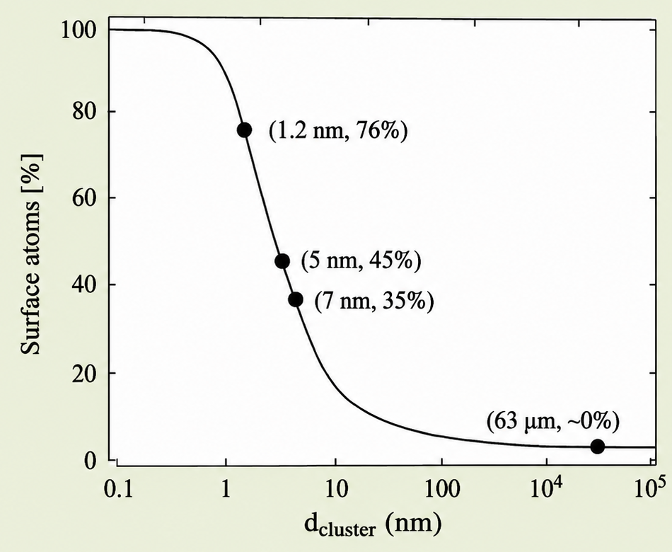
Fig. 4.1 Percentage of surface atoms as a function of palladium cluster diameter (log scale). The curve shows a steep sigmoid transition: above ~100 nm essentially no atoms are surface atoms, while below ~5 nm the majority of atoms reside at the surface. Data points at 1.2 nm (76%), 5 nm (45%), 7 nm (35%), and 63 µm (~0%) bracket the transition. Source: Nutzenadel et al., Eur. Phys. J. D8 (2000) 245; G. Cao.
The practical consequence is profound. Catalytic activity, for example, depends on the availability of surface atoms to bind reactant molecules, break bonds, and facilitate chemical transformation. A catalyst made of 5 nm palladium particles has 45% of its atoms doing useful catalytic work — compared to a fraction of a percent for bulk palladium. This is why supported nanoparticle catalysts can reduce the required loading of precious metals like platinum, palladium, and gold by orders of magnitude compared to bulk or microparticle forms, with no loss of activity. The same logic applies to gas sensing, drug delivery, and photocatalysis: the nanoscale surface is the functional element.
2 Surface Energy Increases Catastrophically with Subdivision
Beyond the fraction of surface atoms, the total surface energy of a material increases dramatically as it is subdivided into smaller pieces. Surface energy is an intrinsic material property — the energy per unit area required to create a new surface by breaking bonds. When a bulk material is divided into progressively smaller particles, the total surface area increases while the total mass remains constant, and so the total surface energy stored in the system rises sharply.
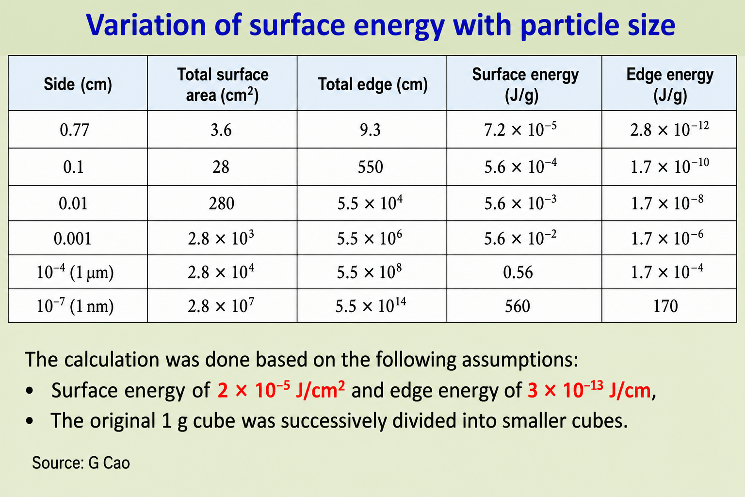
Fig. 4.2 Variation of surface energy and edge energy with particle size for iron cubes subdivided from a 1 g sample. Assumptions: surface energy γ = 2×10⁻⁵ J/cm², edge energy = 3×10⁻¹³ J/cm. As the cube side decreases from 0.77 cm to 1 nm, total surface area increases from 3.6 cm² to 2.8×10⁷ cm², surface energy per gram rises from 7.2×10⁻⁵ J/g to 560 J/g, and edge energy rises from 2.8×10⁻¹² J/g to 170 J/g. Source: G. Cao.
The numbers in this table are striking. Subdividing 1 gram of iron into 1 nm cubes raises the surface energy from a negligible 7.2×10⁻⁵ J/g to 560 J/g — an increase of nearly ten million times. The edge energy (associated with atoms at edges and corners, which have even fewer neighbours than flat surface atoms) rises from 2.8×10⁻¹² J/g to 170 J/g — an increase of roughly 60 billion times. This enormous stored energy is what makes nanoparticles thermodynamically unstable or metastable: the system is always driven to reduce its total surface energy by coarsening — merging small particles into larger ones. Overcoming this thermodynamic driving force is one of the central challenges in the synthesis and stabilisation of nanomaterials.
3 Nanotechnology Is Not a New Phenomenon: The Lycurgus Cup
While nanotechnology as a formal scientific discipline is a product of the late twentieth century, the exploitation of nanoscale phenomena by humans is ancient. The most celebrated historical example is the Lycurgus Cup, a Roman cage cup dating to the 4th century AD and now held in the British Museum. This extraordinary artefact appears jade green when illuminated by reflected light, but transforms to a glowing ruby red when light is transmitted through it — a colour-switching behaviour that puzzled scientists for decades after the cup's rediscovery in modern times.

Fig. 4.3 The Lycurgus Cup (4th century AD, British Museum). In reflected light the cup appears green; in transmitted light it appears red — a dual optical response arising from gold and silver nanoparticles embedded in the glass matrix. The TEM inset (right) shows one such gold nanoparticle approximately 50 nm in diameter embedded within the glass. This is one of the earliest known examples of deliberate (or accidental) exploitation of plasmonic nanoparticle optics. Source: The British Museum.
Analysis of the glass matrix in the 1990s revealed the explanation: the glass contains colloidal gold and silver nanoparticles approximately 50–70 nm in diameter, almost certainly introduced inadvertently through the use of impure gold and silver in the glassmaking process. These nanoparticles exhibit a phenomenon called surface plasmon resonance — the collective oscillation of conduction electrons at the nanoparticle surface driven by incident light — which causes them to absorb and scatter light at specific wavelengths that depend sensitively on particle size, shape, and the dielectric environment. The green reflected colour and red transmitted colour are the direct optical signatures of this plasmonic absorption.
4 Nanomaterials in Art: The Lycurgus Myth and Colloidal Gold
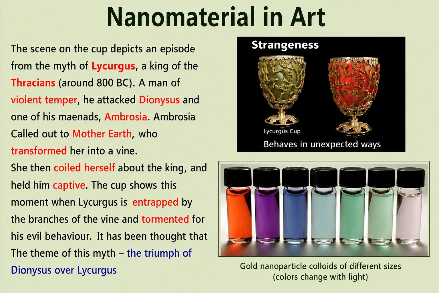
Fig. 4.4 Left: The Lycurgus Cup exhibiting its characteristic dichroic colour change — green in reflected light, red in transmitted light — due to embedded gold-silver nanoparticles. Right: A series of vials containing colloidal gold nanoparticle suspensions of increasing particle diameter, demonstrating the size-dependent colour tuning from red (small particles, ~10–20 nm) through purple to blue-grey (larger particles, ~100 nm). This colour series is a direct visual demonstration of size-tunable surface plasmon resonance.
The scene carved into the Lycurgus Cup depicts an episode from Greek mythology: Lycurgus, a violent king of the Thracians, attacked the god Dionysus and one of his companions, Ambrosia. Ambrosia called upon Mother Earth, who transformed her into a vine that coiled around the king and held him captive, punishing him for his hubris. The triumph of Dionysus over Lycurgus — of the divine and natural over the merely powerful — is rendered in extraordinary detail in the cage-cup carving. That this masterpiece of ancient craftsmanship also contains functional nanoparticles is one of the most remarkable coincidences in the history of materials science.
The series of colloidal gold solutions shown alongside the cup provides a modern demonstration of the same physics. As gold nanoparticle diameter increases from roughly 10 nm to 100 nm, the plasmon resonance peak shifts from green absorption (giving red transmitted colour) through blue-green absorption (giving purple) to red absorption (giving blue). The Romans, working with impure gold compounds, unknowingly produced particles in exactly the size range that gives the characteristic ruby-red transmitted colour. The fact that the same effect can now be reproduced deliberately and tuned across the entire visible spectrum by controlling particle size is a measure of how far nanotechnology has progressed — from accidental art to precision engineering.
5 Surface Plasmon Resonance: The Physical Mechanism
The optical behaviour of the Lycurgus Cup is governed by surface plasmon resonance (SPR), a phenomenon that has become one of the most technologically exploited properties of metallic nanoparticles. To understand SPR, it is necessary to first understand plasmons. In a metal, conduction electrons are not bound to individual atoms but move freely through the lattice — they form a quantum fluid, or plasma, of mobile charge carriers. A plasmon is a quantised collective oscillation of this electron plasma, propagating through the bulk of the metal.
At the surface of a nanoparticle, the electron plasma is spatially confined. When electromagnetic radiation (light) strikes the nanoparticle, its oscillating electric field can drive the surface conduction electrons into resonant collective oscillation — a surface plasmon. In bulk metals, surface plasmons exist but their resonance frequencies are shifted relative to bulk plasmons and they couple only weakly to visible light. In nanoparticles, however, the confinement geometry concentrates the plasmonic response into a sharp resonance that falls squarely within the visible spectrum for noble metals such as gold, silver, and copper.
The resonance frequency — and therefore the colour — depends on nanoparticle size, shape, and the surrounding dielectric medium. Spherical gold nanoparticles of ~20 nm diameter resonate at approximately 520 nm (green absorption → red colour). As size increases, the resonance red-shifts. Non-spherical shapes — rods, triangles, stars — produce multiple resonance peaks and dramatically extended tuning ranges. This tunability is what makes plasmonic nanoparticles so versatile: the same gold chemistry can produce nanoparticles that absorb anywhere from the blue visible to the near-infrared, simply by changing particle geometry.
6 Benjamin Franklin's Monolayer: An Unwitting Nanoscience Experiment

Fig. 4.5 Benjamin Franklin's 1773 letter to William Brownrigg describes what is now recognised as the first quantitative experiment in surface science and nanoscience. Franklin observed that one teaspoon of oil (~5 ml) spread to cover approximately half an acre (~2000 m²) of the Clapham Common pond — implying a film thickness of roughly 2.5 nm, remarkably close to the length of an oleic acid molecule. This is the earliest recorded estimation of molecular dimensions.
In 1773, Benjamin Franklin performed what is now recognised as one of the earliest experiments in surface science — and arguably in nanoscience — without intending to do either. Writing to his friend William Brownrigg, Franklin described pouring a small amount of oil onto the surface of a large pond on Clapham Common in south London. He observed that the oil spread with remarkable speed and extent, eventually calming the wind-ruffled surface of approximately half an acre of the pond.
The quantitative insight that Franklin's observation contains is extraordinary. One teaspoon of oil (approximately 5 ml = 5 cm³) spread over half an acre (approximately 2000 m² = 2×10⁷ cm²). The implied film thickness is therefore 5 cm³ ÷ 2×10⁷ cm² = 2.5×10⁻⁷ cm = 2.5 nm. This is almost exactly the length of an oleic acid molecule — the principal component of olive oil — in its extended conformation. Franklin had, without knowing it, created a monomolecular film and estimated the size of a molecule two centuries before the tools to visualise such things would exist. This experiment is now recognised as the first recorded measurement of a molecular dimension, and Clapham Common — an 89-hectare area of grassland in south London — is commemorated in the history of nanoscience for this reason.
7 Franklin's Experiment as the Basis for Thin Film Technologies
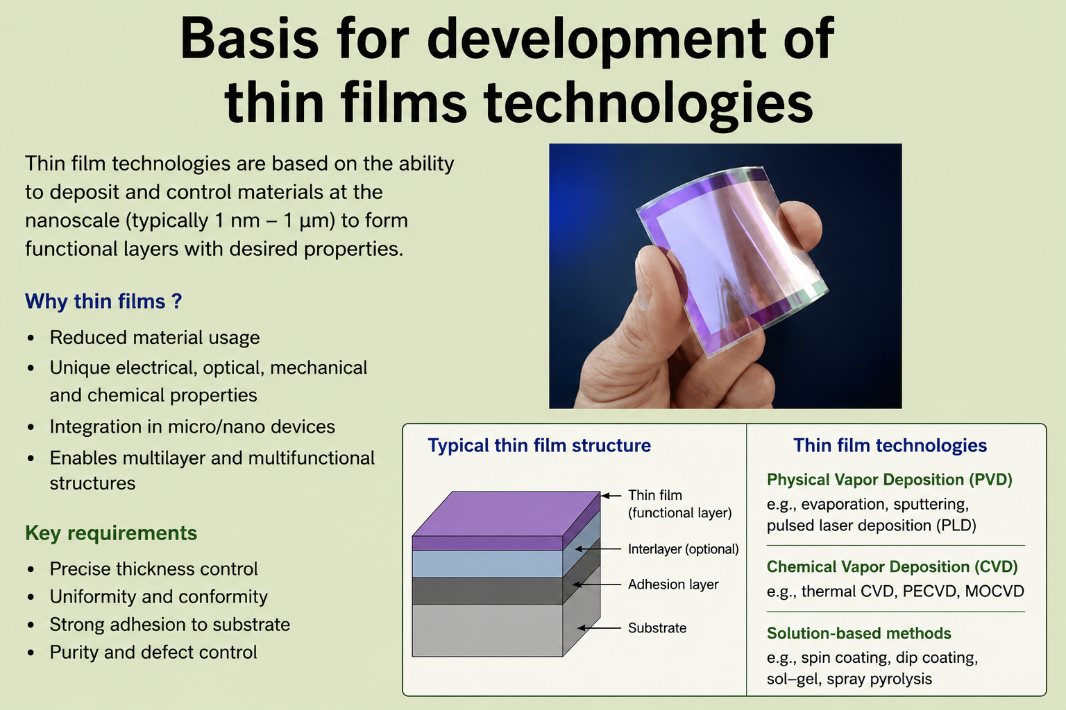
Fig. 4.6 A modern flexible thin film demonstrating the iridescent optical properties that arise from nanoscale film thickness — the same interference effects that make soap bubbles colourful. Franklin's accidental monomolecular film experiment laid the conceptual groundwork for the entire discipline of thin film science, which today encompasses anti-reflection coatings, solar cells, flexible electronics, diffusion barriers, and optical filters.
Franklin's observation that a small volume of oil could spread to create an extremely thin, coherent film over a large area is the conceptual ancestor of the entire thin film technology industry. Thin films — coatings with thickness ranging from a single atomic monolayer up to a few micrometres — are ubiquitous in modern technology. Anti-reflection coatings on camera lenses, hard coatings on cutting tools, transparent conducting layers in solar cells and touchscreens, diffusion barriers in microelectronics packaging, and magnetic layers in hard disk drives are all thin film technologies.
The connection between Franklin's experiment and modern thin film deposition is not merely metaphorical. The Langmuir–Blodgett technique — developed in the 1930s by Irving Langmuir and Katharine Blodgett — directly builds on Franklin's observation by using amphiphilic molecules (molecules with a water-loving head group and an oil-loving tail, like oleic acid) to deliberately assemble monomolecular films on water surfaces and then transfer them layer by layer onto solid substrates. This technique is still used today to produce ultrathin organic coatings with atomic precision.
8 Surface Energy: Definition and Physical Origin
The vast surface energy stored in nanomaterials — as quantified by the subdivision calculation for iron — demands a rigorous physical definition of surface energy and an understanding of its atomic origins. Surface energy arises from a simple but profound asymmetry: atoms at the surface of a solid are in a fundamentally different environment from atoms in the bulk.
In the bulk, every atom is surrounded by its full complement of nearest neighbours — the coordination number characteristic of the crystal structure (12 for FCC, 8 for BCC, 4 for diamond cubic). Each of these neighbour–neighbour interactions contributes a bonding energy that stabilises the atom and lowers the total energy of the system. At the surface, however, the layer of atoms above has been removed. Surface atoms therefore have dangling bonds — unsatisfied valences pointing into the vacuum above the surface. The energy associated with these broken bonds must be supplied from somewhere, and that energy cost is the surface energy.
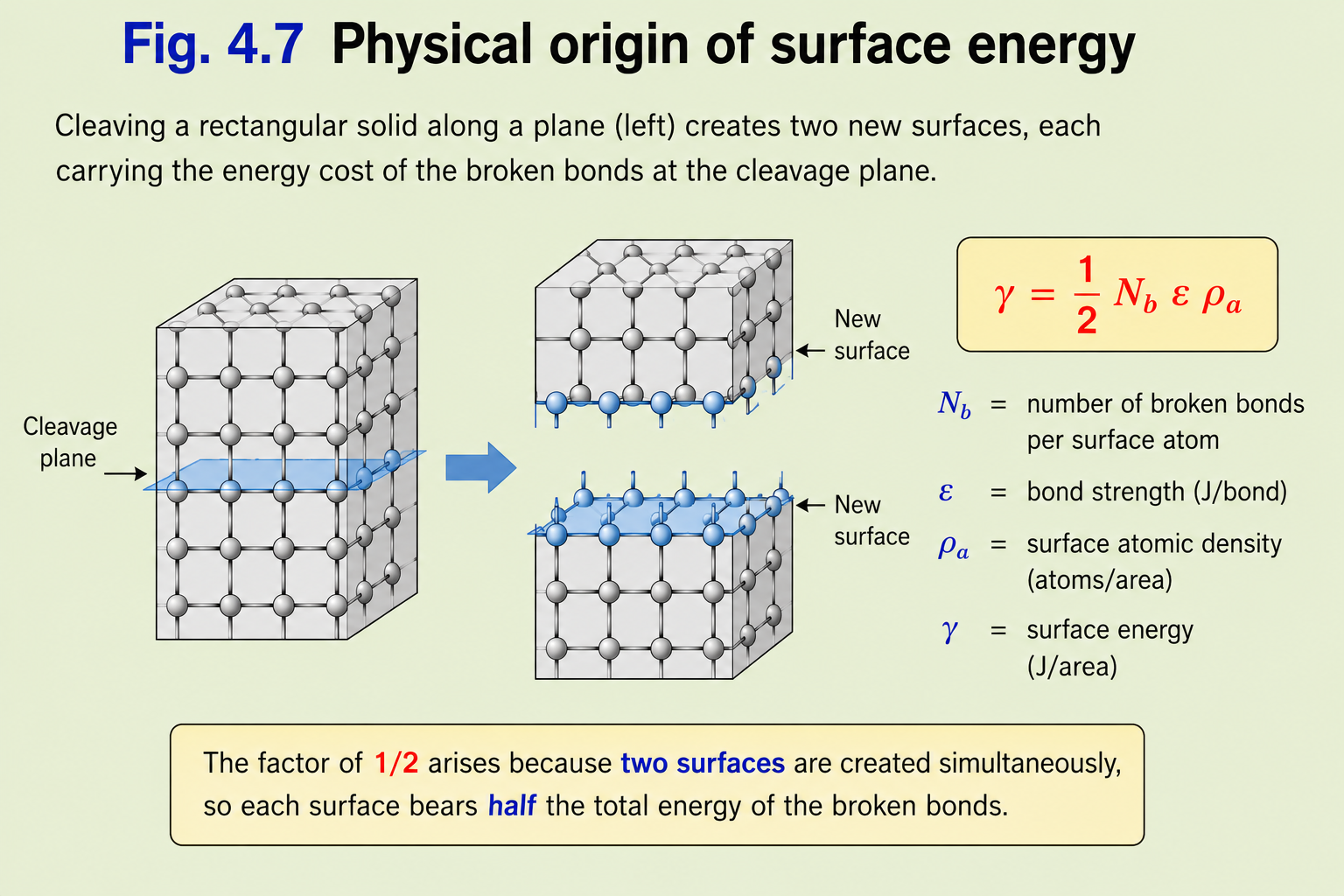
Fig. 4.7 Physical origin of surface energy. Cleaving a rectangular solid along a plane (left) creates two new surfaces, each carrying the energy cost of the broken bonds at the cleavage plane. The surface energy γ is given by γ = ½ Nb ε ρa, where Nb is the number of broken bonds per surface atom, ε is the bond strength (J/bond), and ρa is the surface atomic density (atoms/area). The factor of ½ arises because two surfaces are created simultaneously, so each surface bears half the total energy of the broken bonds.
The equation γ = ½ Nb ε ρa captures this physics in compact form. For a face-centred cubic metal like copper or gold, a (100) surface has Nb = 4 broken bonds per surface atom (out of 12 total nearest neighbours). With known values of ε and ρa from crystal structure data, this gives surface energies in the range of 1–3 J/m² — values consistent with experimental measurements for many metals. The key point is that surface energy scales with the number and strength of the bonds that must be broken to create the surface: high-melting-point metals with strong bonds (tungsten, molybdenum) have high surface energies; low-melting-point metals with weak bonds (tin, indium) have low surface energies.
It is important to recognise that this formula is a simplified model. It ignores higher-order neighbour interactions, assumes that bond strength ε is the same for surface and bulk atoms (which it is not — surface bonds are typically slightly stronger due to electron redistribution), excludes entropic contributions and pressure-volume work, and applies strictly only to solids with perfectly rigid structures where no surface relaxation occurs. Despite these limitations, it provides a reliable order-of-magnitude estimate and the correct physical trends, making it a valuable tool for comparative reasoning about surface energetics.
9 Surface Relaxation and Its Effect on Surface Energy
In real materials, the creation of a surface does not leave the atomic structure unchanged. Surface atoms, deprived of their upper neighbours, experience a net inward force — their remaining bonds pull them toward the bulk, causing the topmost atomic layer to contract inward. This phenomenon is called surface relaxation. In some materials, the surface atoms rearrange laterally as well, forming a new two-dimensional structure that differs from a simple truncation of the bulk lattice — this is called surface reconstruction.
When surface relaxation occurs, the surface atoms move to positions of lower energy than they would occupy in the unrelaxed (bulk-truncated) surface. The dangling bonds are partially satisfied by the inward displacement and by electron redistribution. As a result, the actual surface energy of a relaxed surface is lower than the value predicted by the simple broken-bond model γ = ½ Nb ε ρa. This is not a failure of the model but an expected correction: the model assumes rigid atomic positions, whereas real surfaces are not rigid.
Despite its over-simplified assumptions — ignoring higher-order neighbours, assuming uniform bond strength, excluding entropic and pressure-volume contributions, and neglecting surface relaxation — the broken-bond equation provides reliable general guidance for calculating and comparing surface energies across materials. Its value lies in the physical intuition it encodes: surface energy is proportional to the number and strength of the bonds broken to create the surface, modified by the atomic density of the surface plane.
10 Surface Energy of Low-Index Crystal Faces
Not all surfaces of a crystal have the same surface energy. The energy of a particular crystal face depends on its atomic arrangement — specifically on the number of broken bonds per surface atom, which varies with crystallographic orientation. The faces with the lowest surface energy are those with the highest atomic packing density and the fewest broken bonds per unit area. These are invariably the low-index faces — the {100}, {110}, and {111} planes of cubic crystals — because they correspond to the most closely packed atomic planes in the crystal structure.
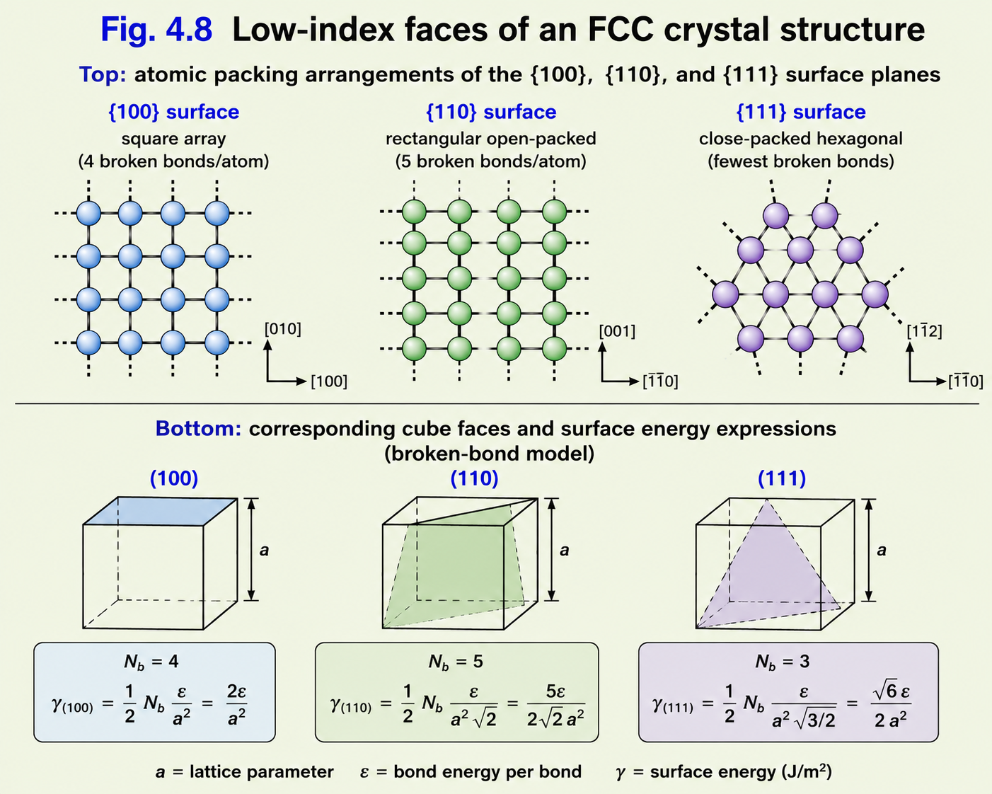
Fig. 4.8 Low-index faces of an FCC crystal structure. Top: atomic packing arrangements of the {100} (square array, 4 broken bonds/atom), {110} (rectangular open-packed, 5 broken bonds/atom), and {111} (close-packed hexagonal, fewest broken bonds) surface planes. Bottom: the corresponding cube faces and surface energy expressions derived from the broken-bond model, with a the lattice parameter and ε the bond energy per bond.
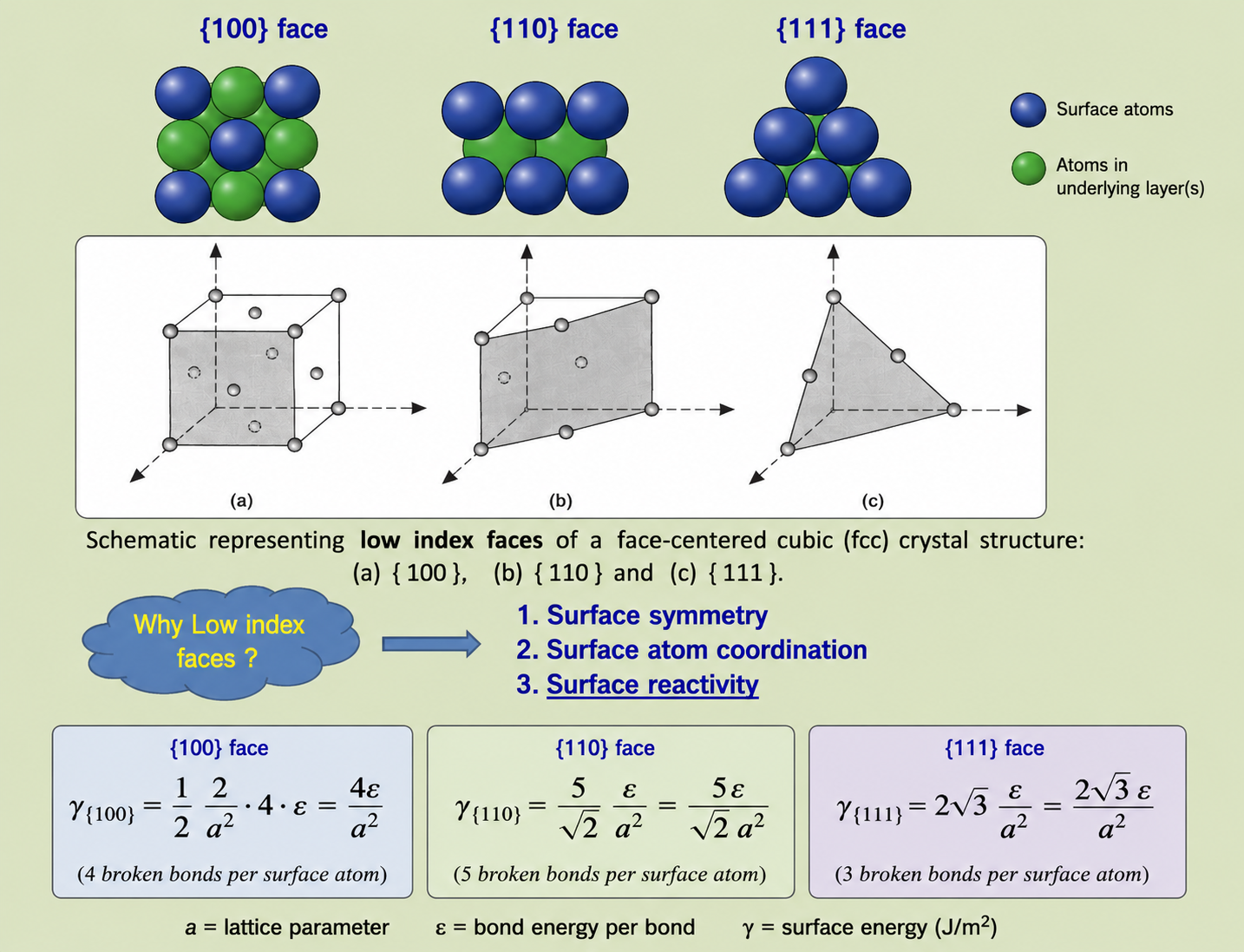
Fig. 4.9 Detailed atomic packing and surface energy for the three principal low-index faces of an FCC crystal. The {100} face has a square atomic arrangement with 4 broken bonds per surface atom, giving γ{100} = 4ε/a². The {110} face is more open, with 5 broken bonds per surface atom and γ{110} = 5ε/(√2·a²). The {111} face is the most densely packed, with the fewest broken bonds and the lowest surface energy γ{111} = 2√3·ε/a². These differences in surface energy govern crystal growth morphology, nanoparticle shape, and catalytic face selectivity.
The three surface energy expressions reveal a clear hierarchy: γ{111} < γ{100} < γ{110} for FCC metals. This ordering has three important consequences. First, it determines surface symmetry — each face has a characteristic 2-D lattice that governs how adsorbates bind and diffuse. Second, it controls surface atom coordination — the number of remaining nearest neighbours per surface atom differs across faces, directly affecting reactivity. Third, it drives surface reactivity: the {110} face, with the most broken bonds, is the most reactive and catalytically active, while {111} is the most stable and least reactive. This is why catalytic selectivity can be controlled by synthesising nanoparticles with specific exposed crystal faces — a practice now known as facet-controlled nanocrystal synthesis.
The equilibrium shape of a crystal — the shape it adopts when given sufficient atomic mobility to minimise total surface energy — is determined by the Wulff construction, which assigns face areas inversely proportional to surface energy. Faces with low surface energy (like {111} in FCC metals) are large and flat; faces with high surface energy (like {110}) are small or absent entirely. Understanding and controlling this Wulff equilibrium shape is central to rational design of catalytic nanoparticles, where the exposed face determines which chemical reactions the particle can accelerate.
Key Takeaways
- The fraction of surface atoms rises steeply as particle size decreases — at 1.2 nm, 76% of palladium atoms are surface atoms, making the material fundamentally surface-dominated.
- Subdividing 1 g of iron into 1 nm cubes increases surface energy by ~10 million times, creating a powerful thermodynamic driving force for coarsening that must be overcome in nanomaterial synthesis.
- The Lycurgus Cup demonstrates that gold and silver nanoparticles have been exploited for their optical properties since the 4th century AD — surface plasmon resonance produces the characteristic green-reflected/red-transmitted dichroism.
- Benjamin Franklin's oil-on-pond experiment (1773) inadvertently created a monomolecular film ~2.5 nm thick — the first recorded estimation of a molecular dimension and the conceptual origin of thin film science.
- Surface energy arises from broken bonds at the surface: γ = ½ Nb ε ρa. This model, while simplified, gives correct physical trends across materials.
- Low-index crystal faces ({100}, {110}, {111} in FCC) have different numbers of broken bonds and therefore different surface energies, governing crystal shape, growth, and catalytic face selectivity.
✦ References & Further Reading
- Cao, G. (2004). Nanostructures & Nanomaterials: Synthesis, Properties & Applications. Imperial College Press.
- Nutzenadel, C. et al. (2000). Scanning tunneling spectroscopy study of metallic clusters. Eur. Phys. J. D, 8, 245.
- Freestone, I. et al. (2007). The Lycurgus Cup — a Roman nanotechnology. Gold Bulletin, 40(4), 270–277.
- Franklin, B. (1774). Of the stilling of waves by means of oil. Phil. Trans. Royal Soc., 64, 445–460.
- Israelachvili, J. N. (2011). Intermolecular and Surface Forces (3rd ed.). Academic Press.
- Wulff, G. (1901). Zur Frage der Geschwindigkeit des Wachstums und der Auflösung der Krystallflächen. Z. Kristallogr., 34, 449–530.
Surface Stabilisation & Chemical Potential
From surface relaxation and restructuring to Ostwald ripening and the Young–Laplace equation — the mechanisms by which nanomaterials minimise their surface energy.
Contents
- Low-Index Faces and Crystal Growth Direction in Silicon
- Thermodynamic Driving Force: Minimisation of Total Surface Energy
- Atomic-Level Mechanisms: Relaxation, Restructuring, and Adsorption
- System-Level Mechanisms: Agglomeration, Sintering, and Ostwald Ripening
- Chemical Potential as a Function of Surface Curvature
- References & Further Reading
1 Low-Index Faces and Crystal Growth Direction in Silicon
Building on the surface energy hierarchy established for FCC metals, it is instructive to examine a technologically critical non-FCC material: silicon. Silicon belongs to the cubic crystal system but adopts the diamond cubic structure — a framework of two interpenetrating FCC lattices offset by one-quarter of the body diagonal, giving each silicon atom four tetrahedral nearest neighbours. This tetrahedral bonding geometry is the structural origin of silicon's semiconductor properties and its characteristic cleavage behaviour.
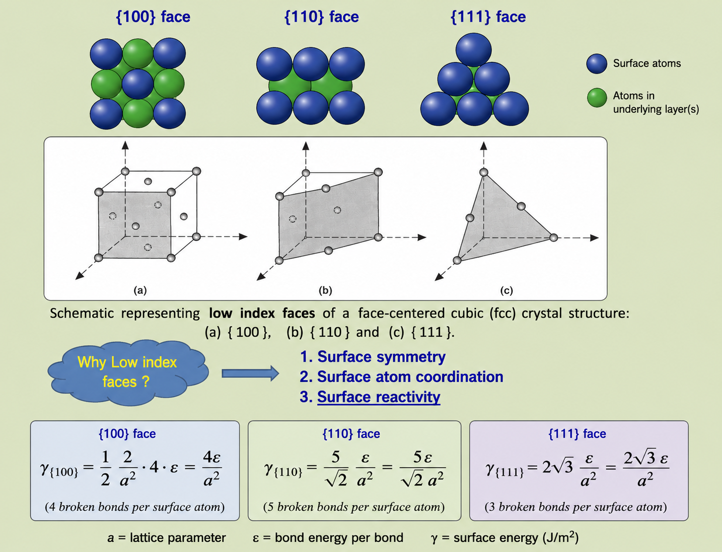
Fig. 5.1 Low-index faces of an FCC crystal — the {100}, {110}, and {111} planes shown with their atomic packing arrangements and surface energy expressions. The {111} face has the lowest surface energy in FCC metals, which directly governs preferred crystal growth directions and nanoparticle equilibrium shapes.
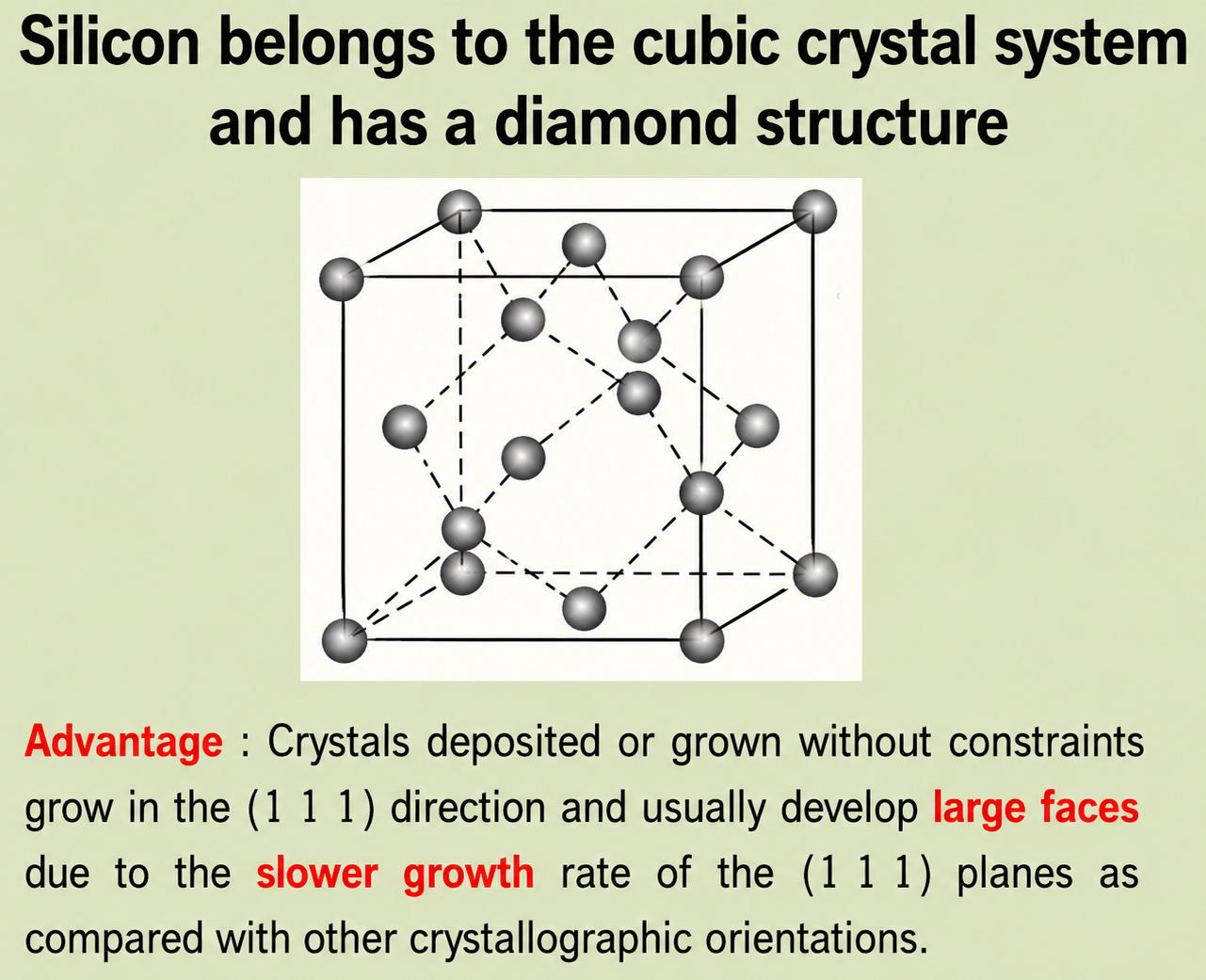
Fig. 5.2 The diamond cubic crystal structure of silicon. Each atom is tetrahedrally coordinated with four nearest neighbours at bond angles of 109.5°. The structure consists of two interpenetrating FCC lattices displaced by (¼, ¼, ¼)a along the body diagonal, where a = 0.543 nm is the lattice parameter. The {111} planes in this structure are the most densely packed and carry the lowest surface energy.
In silicon, crystals deposited or grown without external constraints preferentially grow in the ⟨111⟩ direction. This occurs because the (111) planes have the slowest growth rate — they are the most stable, lowest-energy faces, and the crystal therefore exposes large, well-developed {111} facets. This anisotropic growth behaviour is not merely of academic interest: it is the foundation of silicon wafer technology. Single-crystal silicon boules are deliberately grown along specific crystallographic orientations (⟨100⟩ or ⟨111⟩) to control the cleavage plane, dopant distribution, and oxidation rate of the resulting wafers. The {111} wafer orientation, historically preferred for bipolar transistors, cleaves cleanly along {111} planes; the {100} orientation, now dominant for CMOS technology, provides a faster and more controllable thermal oxidation rate and lower interface state density at the Si/SiO₂ interface.
2 Thermodynamic Driving Force: Minimisation of Total Surface Energy
Every process in materials science is ultimately governed by thermodynamics. The direction of spontaneous change is always toward lower free energy. For a system containing surfaces — whether a nanoparticle suspension, a thin film, or a polycrystalline solid — the relevant contribution to the Gibbs free energy includes a surface energy term. Because surface energy is always positive (creating new surface always costs energy), thermodynamics drives the system to minimise the total surface area for a given volume of material.
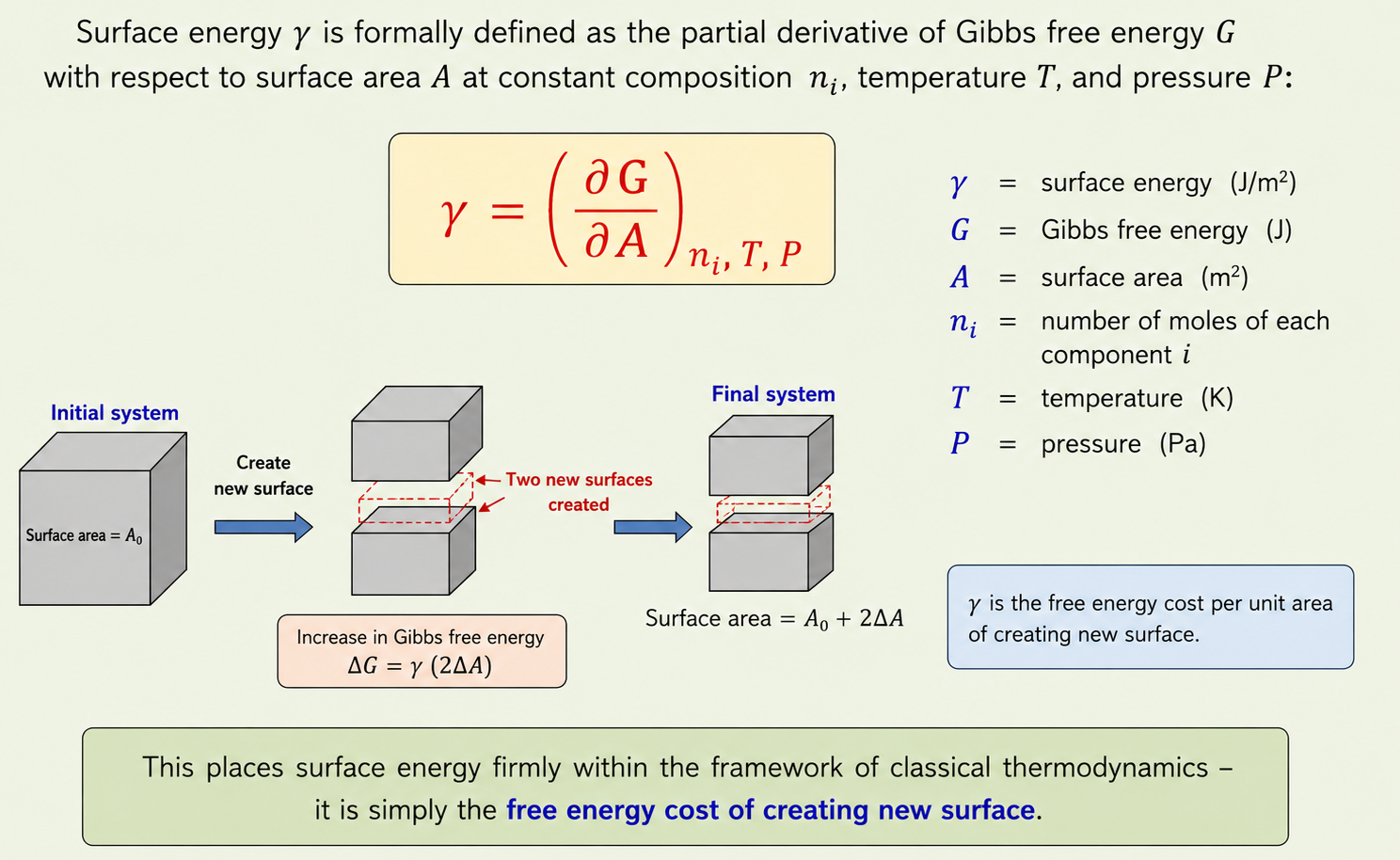
Fig. 5.3 Thermodynamic definition of surface energy. Surface energy γ is formally defined as the partial derivative of Gibbs free energy G with respect to surface area A at constant composition ni, temperature T, and pressure P: γ = (∂G/∂A)ni,T,P. This places surface energy firmly within the framework of classical thermodynamics — it is simply the free energy cost of creating new surface.
The formal thermodynamic definition of surface energy is γ = (∂G/∂A)ni,T,P — the rate of change of Gibbs free energy with surface area at constant composition, temperature, and pressure. This definition is more general than the broken-bond model encountered in the previous lecture: it includes not just the enthalpic cost of broken bonds but also entropic contributions from surface disorder, adsorbed species, and thermal vibrations. At room temperature the entropic term is relatively small for most solid surfaces, so the broken-bond estimate is reasonable; at elevated temperatures, however, entropic effects become significant and γ decreases with increasing temperature, which is why surfaces and grain boundaries become more mobile at high temperature.
The thermodynamic imperative to minimise total surface energy drives three broad classes of phenomena in nanomaterials: atomic-level surface rearrangements, shape changes of individual nanostructures, and coarsening at the system level through particle merging or growth. Understanding these mechanisms is essential for designing stable nanomaterials that retain their properties under processing and service conditions.
3 Atomic-Level Mechanisms: Relaxation, Restructuring, and Adsorption
At the atomic or surface level, three principal mechanisms operate to reduce the surface energy of a given surface with fixed area. Each represents a different strategy for satisfying the dangling bonds of surface atoms.
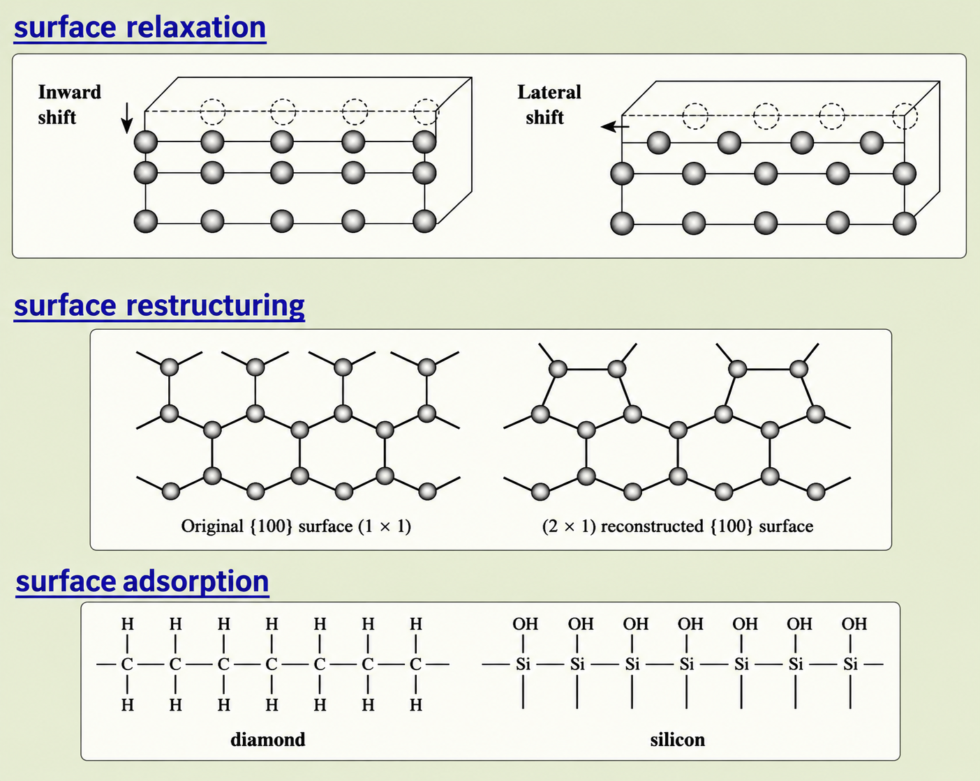
Fig. 5.4 Three atomic-level mechanisms for surface energy reduction. Surface relaxation (top): surface atoms shift inward (normal relaxation) or laterally to reduce dangling bond energy — more common in liquids, limited in rigid solids. Surface restructuring (middle): original {100} surface atoms pair up to form new strained bonds in a (2×1) reconstruction, reducing the number of dangling bonds at the cost of elastic strain energy. Surface adsorption (bottom): dangling bonds on diamond (terminated by H) and silicon (terminated by OH groups) are chemically satisfied by adsorbates, dramatically reducing surface energy.
Surface relaxation is the simplest mechanism: surface atoms shift their positions — typically inward toward the bulk (normal relaxation) or laterally within the surface plane — to reduce the energy of their dangling bonds through partial re-bonding with subsurface atoms. This process occurs more readily in liquids (where atomic mobility is high) than in crystalline solids (where the rigid lattice constrains movement), but it is observed in all crystalline surfaces to some degree. The magnitude of relaxation is typically a few percent of the interlayer spacing.
Surface restructuring (or surface reconstruction) goes further: surface atoms rearrange into an entirely new two-dimensional periodicity that differs from a simple truncation of the bulk lattice. The classic example shown is the Si(100)-(2×1) reconstruction, in which pairs of surface silicon atoms form dimers — new covalent bonds across the surface — halving the number of dangling bonds at the cost of introducing some compressive strain. The (2×1) notation indicates that the surface unit cell is twice as large as the bulk-truncated unit cell in one direction. Gold (110) undergoes a (1×2) missing-row reconstruction; the (7×7) reconstruction of Si(111) is one of the most complex surface structures known.
Surface adsorption is arguably the most technologically important mechanism. Chemical species from the surrounding environment — gases, liquids, or solids in contact with the surface — bond to the dangling surface bonds, replacing the high-energy vacuum interface with a lower-energy adsorbate-covered surface. The two examples shown are particularly instructive: the diamond surface terminates its carbon dangling bonds with hydrogen atoms (H-termination), and the silicon surface terminates with hydroxyl groups (–OH) in the presence of water or oxygen. Both processes dramatically reduce surface energy. H-termination of silicon is the basis of the HF etching step used in semiconductor processing: immersing a native-oxide-covered silicon wafer in dilute HF removes the oxide and leaves a hydrogen-terminated, atomically smooth, hydrophobic silicon surface that is chemically passivated against further oxidation for minutes to hours.
Composition segregation or impurity enrichment represents a fourth atomic-level mechanism: solute atoms or impurities that have lower surface energy than the host atoms preferentially migrate to the surface through solid-state diffusion, effectively coating the surface with a low-energy layer. This phenomenon is well known in metallurgy — sulphur segregates to iron grain boundaries, bismuth to copper boundaries — and has been observed in nanomaterials as well. The difficulty of doping nanocrystals and the tendency of dopant atoms to be expelled from the nanocrystal interior to its surface is a direct manifestation of this segregation driving force.
4 System-Level Mechanisms: Agglomeration, Sintering, and Ostwald Ripening
Beyond atomic-level surface modifications, the total surface energy of a collection of nanoparticles can be reduced far more dramatically by reducing the number of particles — merging many small particles into fewer large ones. Since surface area scales as the square of particle radius while volume scales as the cube, combining two particles of radius r into one particle of radius 21/3r ≈ 1.26r reduces total surface area by a factor of 21/3 ≈ 1.26 — a 21% reduction per doubling event. Repeated coarsening events rapidly reduce the total surface area and stored surface energy of the system.
Two distinct physical mechanisms drive this system-level coarsening: sintering and Ostwald ripening.
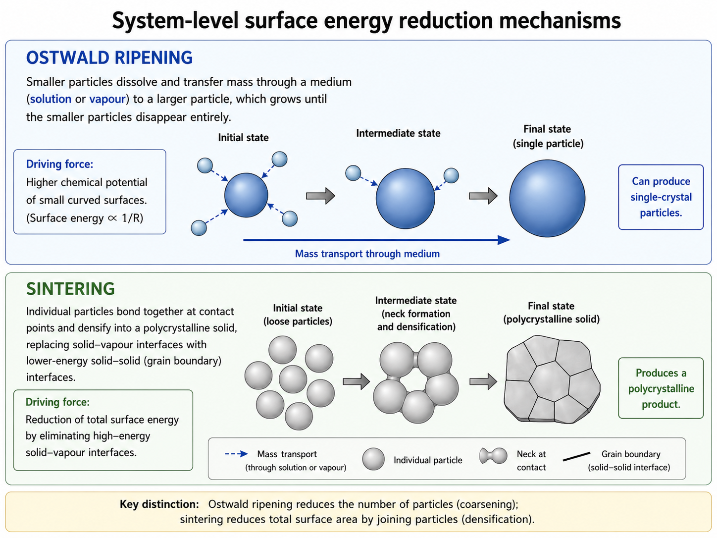
Fig. 5.5 System-level surface energy reduction mechanisms. Ostwald ripening (top): smaller particles dissolve and transfer mass through a medium (solution or vapour) to a larger particle, which grows until the smaller particles disappear entirely. The driving force is the higher chemical potential of small curved surfaces. Sintering (bottom): individual particles bond together at contact points and densify into a polycrystalline solid, replacing solid–vapour interfaces with lower-energy solid–solid (grain boundary) interfaces. Sintering produces a polycrystalline product; Ostwald ripening can produce single-crystal particles.
Sintering involves the bonding of individual nanostructures at their contact points, followed by mass transport (via surface diffusion, grain boundary diffusion, or lattice diffusion) that densifies the aggregate into a solid polycrystalline material. Solid–vapour interfaces at the original particle surfaces are replaced by solid–solid grain boundary interfaces, which have significantly lower energy per unit area. The driving force is therefore the energy difference between the solid–vapour surface energy (γsv ≈ 1–3 J/m² for metals) and the grain boundary energy (γgb ≈ 0.3–1 J/m²). Sintering of conventional powders typically requires temperatures above 70% of the absolute melting point — a rule of thumb known as the homologous temperature criterion. For nanoparticles, however, sintering can begin at dramatically lower temperatures because the extremely high surface energy provides additional driving force and because the diffusion distances are nanometric. This "low-temperature sintering" of nanoparticles is a critical challenge in the processing of nanomaterials: a nanoparticle dispersion that is stable at room temperature may sinter catastrophically at temperatures well below those that would affect the bulk material. The product of sintering is always a polycrystalline material — the grain boundaries between the former individual particles are preserved as structural features in the sintered body.
Ostwald ripening operates by a fundamentally different mechanism. Rather than direct contact between particles, mass is transferred through an intermediate phase — typically a solution or vapour — from smaller particles to larger ones. The driving force is the difference in chemical potential between particles of different curvature: smaller particles have higher surface curvature, higher chemical potential, and therefore higher solubility or vapour pressure than larger particles. Atoms or molecules dissolve preferentially from small particles and deposit preferentially onto large particles, causing the large to grow and the small to shrink and ultimately disappear. The process continues until all particles have reached the same size — in practice, until a broad size distribution narrows and the mean particle size grows over time following a characteristic t1/3 power law (the Lifshitz–Slyozov–Wagner or LSW theory). Unlike sintering, Ostwald ripening does not require particle contact and can occur at moderate temperatures in solution-phase systems. It is the primary mechanism of particle growth in colloidal synthesis and is a major challenge in the long-term stability of nanoparticle catalysts, quantum dot displays, and drug delivery systems.
5 Chemical Potential as a Function of Surface Curvature
The thermodynamic basis for Ostwald ripening — and for many other curvature-dependent phenomena in nanomaterials — is the relationship between surface curvature and chemical potential. Intuitively, atoms at a highly curved (small radius) surface are less well bonded than atoms at a flat surface: they have fewer neighbours and more exposure to the environment. This reduced bonding manifests as a higher chemical potential — a greater tendency for those atoms to leave the surface and transfer to a lower-energy environment.
To derive this relationship quantitatively, consider the transfer of dn atoms from an infinite flat surface (chemical potential μ∞) to a spherical solid particle of radius R (chemical potential μc). The volume change of the spherical particle upon receiving dn atoms is:
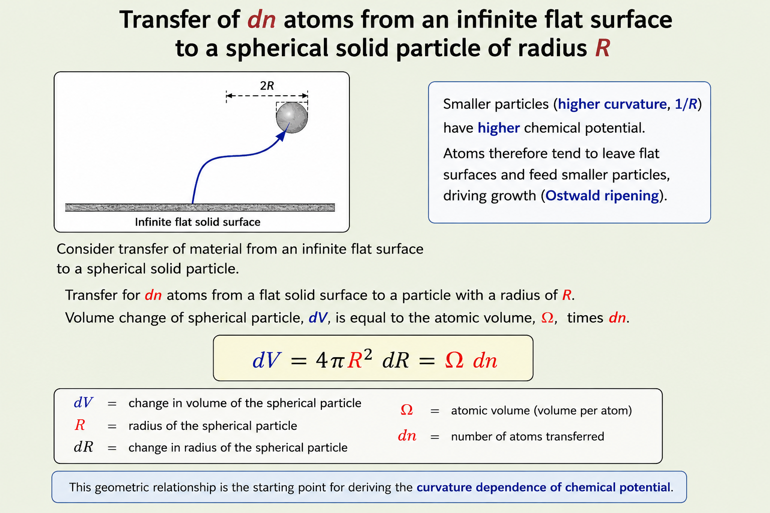
Fig. 5.6 Transfer of dn atoms from an infinite flat surface to a spherical solid particle of radius R. The volume change of the sphere upon receiving dn atoms is dV = 4πR² dR = Ω dn, where Ω is the atomic volume. This geometric relationship is the starting point for deriving the curvature dependence of chemical potential.
The volume change equation dV = 4πR² dR = Ω dn simply states that the increase in sphere volume equals the number of transferred atoms times the volume per atom (atomic volume Ω). From this, the change in surface area upon transferring dn atoms is dA = 8πR dR. The work done per atom transferred — which equals the change in chemical potential Δμ = μc − μ∞ — is the surface energy γ times the rate of change of surface area with atom number:
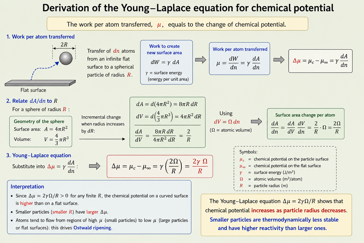
Fig. 5.7 Derivation of the Young–Laplace equation for chemical potential. The work per atom transferred from flat surface to curved particle, Δμ = μc − μ∞ = γ(dA/dn), simplifies to Δμ = 2γΩ/R. This fundamental result shows that chemical potential increases as particle radius decreases — smaller particles are thermodynamically less stable and have higher reactivity than larger ones.
Substituting dA = 8πR dR and dV = 4πR² dR = Ω dn, the result simplifies to the celebrated Young–Laplace equation for chemical potential:
Δμ = μc − μ∞ = 2γΩ / R
where γ is the surface energy, Ω is the atomic volume, and R is the particle radius. The equation shows that the excess chemical potential of atoms on a curved surface over those on a flat reference surface is inversely proportional to the radius of curvature.
The physical implications of this equation are far-reaching. First, it quantitatively explains Ostwald ripening: a particle of radius R = 2 nm has a chemical potential excess over a flat surface that is ten times larger than a particle of R = 20 nm. The smaller particle is thermodynamically driven to dissolve and transfer its atoms to the larger one. Second, it explains the size-dependent solubility of nanoparticles — the Gibbs–Thomson or Ostwald–Freundlich equation, which shows that smaller particles have exponentially higher solubility in a surrounding medium. Third, it governs vapour pressure above nanoparticles (the Kelvin equation), the critical nucleus size in nucleation theory, the capillary condensation of liquids in nanopores, and the melting point depression of nanoparticles. All of these phenomena — diverse as they appear — are unified by the same underlying physics: curvature raises chemical potential, and the effect scales as 1/R.
- Ostwald ripening: smaller particles (higher μ) dissolve; larger particles (lower μ) grow — drives particle size coarsening over time.
- Gibbs–Thomson effect: solubility of a particle increases as size decreases — nanoparticles are more soluble than bulk material.
- Kelvin equation: vapour pressure above a curved liquid droplet or solid particle is higher than above a flat surface — relevant to aerosol formation and nanoscale evaporation.
- Nucleation theory: a critical nucleus radius R* exists below which nuclei dissolve and above which they grow — governed by the balance between volume free energy gain and surface energy cost.
- Melting point depression: nanoparticles melt at lower temperatures than bulk because the high surface-to-volume ratio makes the surface energy contribution to total free energy significant.
Key Takeaways
- Silicon's diamond cubic structure causes preferential growth in the ⟨111⟩ direction due to the lowest surface energy of {111} planes — the same principle governs silicon wafer orientation selection in semiconductor manufacturing.
- Surface energy is formally γ = (∂G/∂A)n,T,P — thermodynamics drives all surfaces and interfaces to minimise total surface area and energy.
- Four atomic-level mechanisms reduce surface energy: surface relaxation (inward/lateral atomic shifts), surface restructuring (new 2-D periodicity, e.g. Si(100)-(2×1)), surface adsorption (chemical termination of dangling bonds), and composition segregation (impurity enrichment at the surface).
- At the system level, sintering (particle bonding and densification at contact points, producing a polycrystalline solid) and Ostwald ripening (dissolution of small particles and growth of large ones via a medium) reduce total surface energy by reducing the number and total area of particle surfaces.
- The Young–Laplace equation Δμ = 2γΩ/R quantifies how chemical potential increases with surface curvature — smaller particles have higher chemical potential, higher solubility, higher vapour pressure, and lower melting points than larger ones. This single equation underpins Ostwald ripening, nucleation theory, the Kelvin equation, and melting point depression in nanomaterials.
✦ References & Further Reading
- Cao, G. (2004). Nanostructures & Nanomaterials: Synthesis, Properties & Applications. Imperial College Press.
- Adamson, A. W. & Gast, A. P. (1997). Physical Chemistry of Surfaces (6th ed.). Wiley-Interscience.
- Lifshitz, I. M. & Slyozov, V. V. (1961). The kinetics of precipitation from supersaturated solid solutions. J. Phys. Chem. Solids, 19(1–2), 35–50.
- Kelvin, Lord (W. Thomson) (1871). On the equilibrium of vapour at a curved surface of liquid. Phil. Mag., 42, 448–452.
- Zhao, M. & Bharat, B. (2003). Nanoscience and nanotechnology in surface phenomena. Ultramicroscopy, 97, 377–389.
- Pimpinelli, A. & Villain, J. (1998). Physics of Crystal Growth. Cambridge University Press.
Kelvin Equation, Gibbs–Thomson & Ostwald Ripening
Principal radii of curvature, the Kelvin and Gibbs–Thomson equations, Ostwald ripening from first principles, and the strategies for stabilising nanomaterials against coarsening.
Contents
- Generalising Chemical Potential to Arbitrary Curved Surfaces
- Vapour Pressure Above Curved Surfaces: Derivation
- The Kelvin and Gibbs–Thomson Equations
- Ostwald Ripening: Mechanism from the Gibbs–Thomson Equation
- Ostwald Ripening in Detail: The Full Schematic
- Stabilisation of Nanomaterials Against Coarsening
- References & Further Reading
1 Generalising Chemical Potential to Arbitrary Curved Surfaces
In the previous lecture, the Young–Laplace equation was derived for the specific case of a spherical particle of radius R, yielding Δμ = 2γΩ/R. A sphere is the simplest curved surface, characterised by a single radius of curvature that is the same in every direction. Real surfaces — the facets of nanocrystals, the tips of nanowires, the menisci of liquids in nanopores — are more complex. Their curvature varies from point to point and is generally described by two independent principal radii of curvature, R1 and R2, measured in two orthogonal planes through the surface normal.
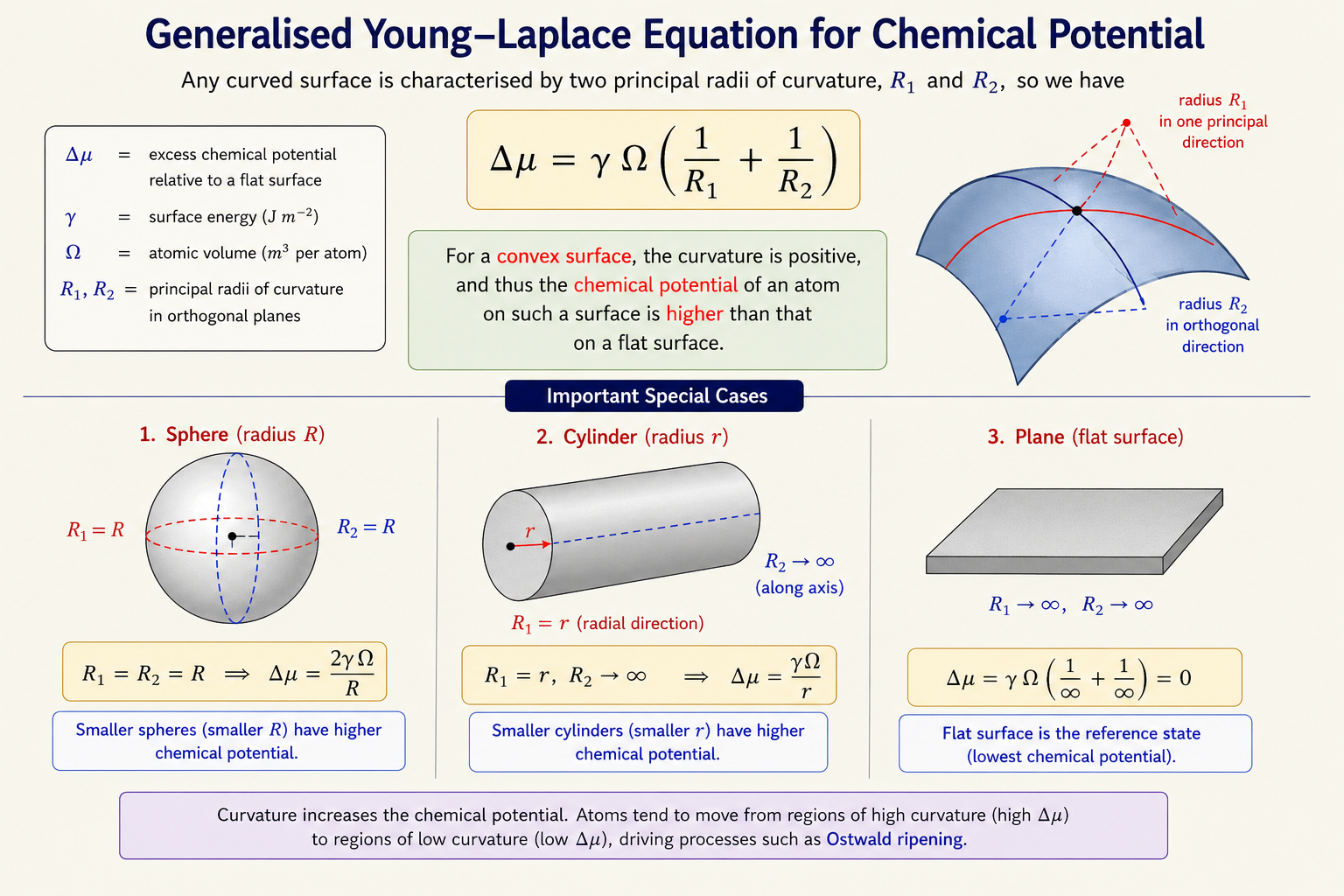
Fig. 6.1 Generalised Young–Laplace equation for chemical potential. Any curved surface is characterised by two principal radii of curvature R1 and R2 in orthogonal planes. The excess chemical potential of an atom on this surface relative to a flat reference is Δμ = γΩ(1/R1 + 1/R2). For a sphere, R1 = R2 = R, recovering Δμ = 2γΩ/R. For a cylinder of radius r, R1 = r and R2 → ∞, giving Δμ = γΩ/r.
The generalised equation Δμ = γΩ(1/R1 + 1/R2) encapsulates a sign convention of critical physical importance. For a convex surface — one that curves away from the material, like the outer surface of a sphere or the tip of a needle — both radii of curvature are positive by convention, so Δμ > 0. Atoms on a convex surface have higher chemical potential than atoms on a flat surface: they are less stably bonded and more reactive. For a concave surface — one that curves into the material, like the interior of a bowl or a surface pit — one or both radii take negative values, and Δμ < 0. Atoms on a concave surface are more stable than atoms on a flat surface: they are better coordinated, having neighbours on more sides.
This sign dependence has profound practical consequences. Mass spontaneously flows from convex regions (high μ) to concave regions (low μ). In a sintering neck between two particles, the saddle-shaped neck region has one positive and one negative radius of curvature; the net curvature can be negative, making the neck a thermodynamic sink that draws material from the convex particle surfaces. This is precisely the mechanism that drives neck growth and densification during sintering. Similarly, during crystal growth, a concave pit on a surface grows preferentially because incoming atoms gain energy by filling the lower-μ concave site.
2 Vapour Pressure Above Curved Surfaces: Derivation
The curvature-dependent chemical potential translates directly into a curvature-dependent vapour pressure — a relationship of enormous importance for understanding nanoparticle stability, aerosol physics, and nanoscale condensation. The derivation proceeds by equating the chemical potential of an atom in the vapour phase with its chemical potential on the solid surface, at equilibrium.
For a flat solid surface in equilibrium with its vapour, the chemical potentials of the vapour atom (μv) and the surface atom (μ∞) are equal. Assuming the vapour obeys the ideal gas law, the chemical potential of a vapour atom is related to the equilibrium vapour pressure P∞ above the flat surface by:
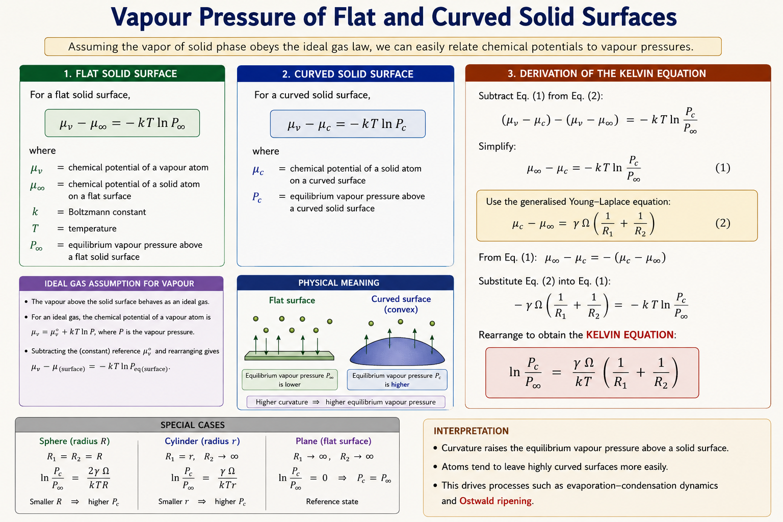
Fig. 6.2 Vapour pressure equations for flat and curved solid surfaces, derived assuming ideal gas behaviour of the vapour phase. For a flat surface: μv − μ∞ = −kT ln P∞. For a curved surface: μv − μc = −kT ln Pc, where Pc is the equilibrium vapour pressure above the curved surface. Subtracting and substituting the Young–Laplace equation yields the Kelvin equation.
For a curved solid surface in equilibrium with its vapour, the chemical potential of surface atoms is elevated by Δμ = γΩ(1/R1 + 1/R2) above the flat surface value. At equilibrium, the vapour above the curved surface must also have this elevated chemical potential, which — through the ideal gas relationship — corresponds to a higher equilibrium vapour pressure Pc above the curved surface than P∞ above the flat surface. Subtracting the two equations and substituting the Young–Laplace expression for Δμ yields the complete derivation of the Kelvin equation.
3 The Kelvin and Gibbs–Thomson Equations
Combining the vapour-phase chemical potential equations with the Young–Laplace expression for surface curvature yields two of the most important equations in nanoscale thermodynamics: the Kelvin equation (relating vapour pressure to curvature) and the Gibbs–Thomson equation (relating solubility to curvature).
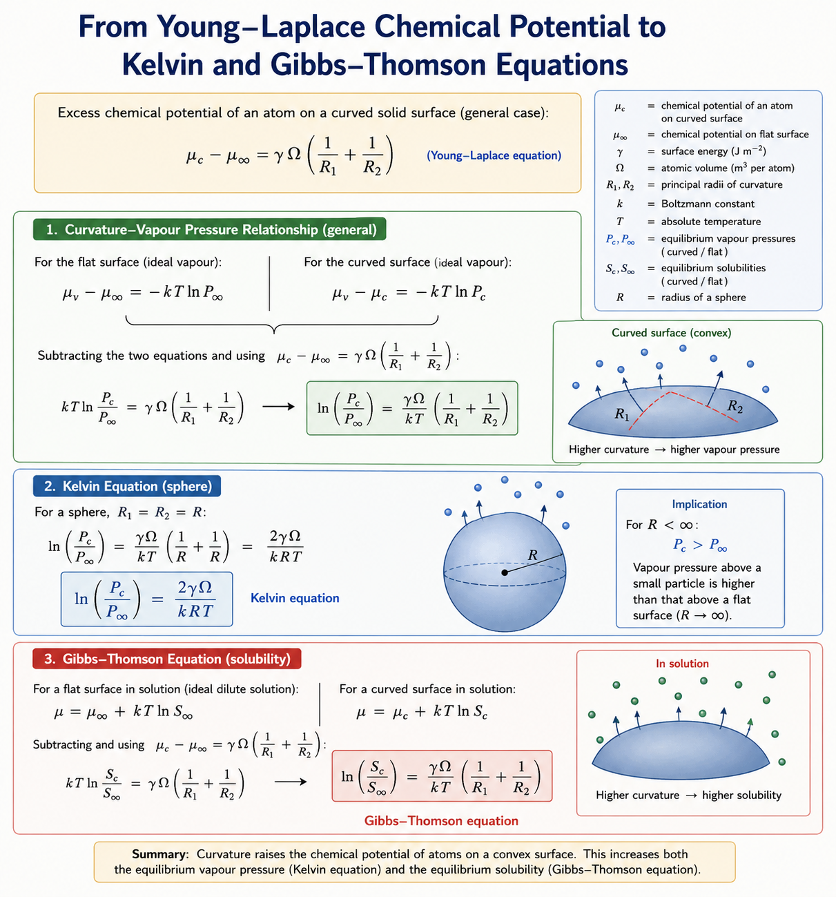
Fig. 6.3 Derivation of the Kelvin and Gibbs–Thomson equations from the Young–Laplace chemical potential. Top: the general curvature–vapour pressure relationship. Middle: the Kelvin equation for a sphere, ln(Pc/P∞) = 2γΩ/kRT, showing that vapour pressure above a spherical particle of radius R exceeds that above a flat surface. Bottom: the Gibbs–Thomson equation, ln(Sc/S∞) = γΩ(R1−1 + R2−1)/kT, showing the same curvature dependence applies to solubility Sc relative to bulk solubility S∞.
ln(Pc/P∞) = 2γΩ / kRT
The equilibrium vapour pressure Pc above a spherical solid particle of radius R is greater than the vapour pressure P∞ above a flat surface of the same material. The enhancement increases exponentially as R decreases: a 2 nm gold nanoparticle has a vapour pressure orders of magnitude higher than bulk gold at the same temperature.
ln(Sc/S∞) = γΩ(R1−1 + R2−1) / kT
The equilibrium solubility Sc of a solid particle with principal radii of curvature R1 and R2 exceeds the bulk solubility S∞ by an amount that increases exponentially with curvature. Smaller particles are intrinsically more soluble than larger ones — a direct thermodynamic consequence of their higher surface-to-volume ratio and elevated chemical potential.
The Kelvin and Gibbs–Thomson equations are structurally identical — both express the logarithmic ratio of a size-dependent intensive property (vapour pressure or solubility) to its bulk value as a linear function of the sum of principal curvatures. This universality reflects the fact that both vapour pressure and solubility are thermodynamic quantities that couple directly to chemical potential: if chemical potential is elevated by curvature, so are both. The practical implication is that any process governed by local concentration gradients in a vapour or solution — evaporation, condensation, dissolution, precipitation, crystal growth — will be sensitive to the curvature of the surfaces involved, and this sensitivity becomes extreme at the nanoscale.
4 Ostwald Ripening: Mechanism from the Gibbs–Thomson Equation
The Gibbs–Thomson equation provides a rigorous thermodynamic foundation for the Ostwald ripening phenomenon introduced in the previous lecture. Consider two solid particles of different radii, R1 >> R2, immersed in a solvent. Each particle establishes a local equilibrium concentration of dissolved material in the surrounding solvent — its solubility — determined by the Gibbs–Thomson equation. Because R2 < R1, particle 2 (the smaller one) has a higher curvature and therefore a higher equilibrium solubility than particle 1.
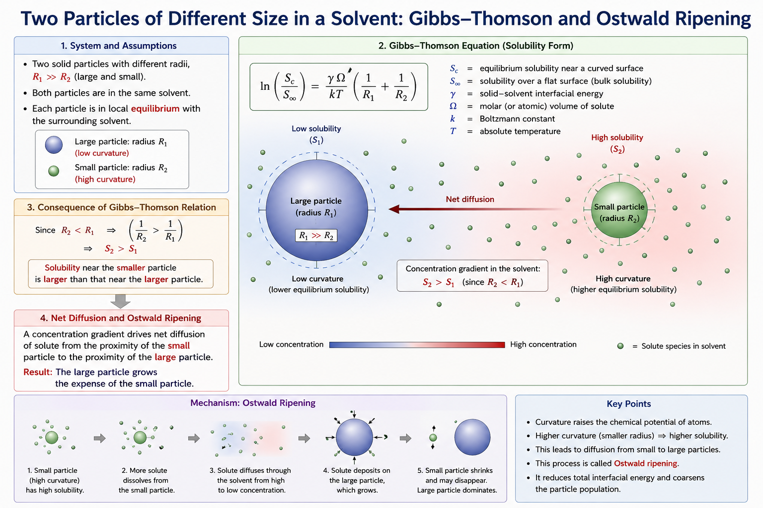
Fig. 6.4 Application of the Gibbs–Thomson equation to two particles of different sizes (R1 >> R2) in a solvent. The smaller particle (larger curvature) has higher equilibrium solubility. A concentration gradient develops in the solvent between the high-concentration region near the small particle and the low-concentration region near the large particle, driving net diffusion of solute from small to large — the fundamental mechanism of Ostwald ripening.
In the region of solvent immediately surrounding the small particle, the local dissolved concentration is elevated to Sc(R2). In the region surrounding the large particle, the local concentration is Sc(R1) < Sc(R2). This spatial concentration gradient drives Fickian diffusion of dissolved material from the neighbourhood of the small particle toward the neighbourhood of the large particle. To maintain local equilibrium, the small particle must continue dissolving (its surrounding concentration would otherwise drop below Sc(R2)), while the large particle must continue growing by precipitation of the arriving solute (its surrounding concentration would otherwise rise above Sc(R1)).
The net result is a continuous transfer of mass from small particles to large particles through the solution phase — without any physical contact between the particles. The small particle shrinks and eventually disappears; the large particle grows. As the small particle shrinks, its radius decreases, its curvature increases, and its solubility increases further — accelerating the process in a self-reinforcing feedback loop. This same mechanism operates whether the transfer medium is a liquid (dissolution–diffusion–precipitation), a gas (evaporation–diffusion–condensation), or even a solid (surface diffusion or grain boundary diffusion at elevated temperatures).
5 Ostwald Ripening in Detail: The Full Schematic
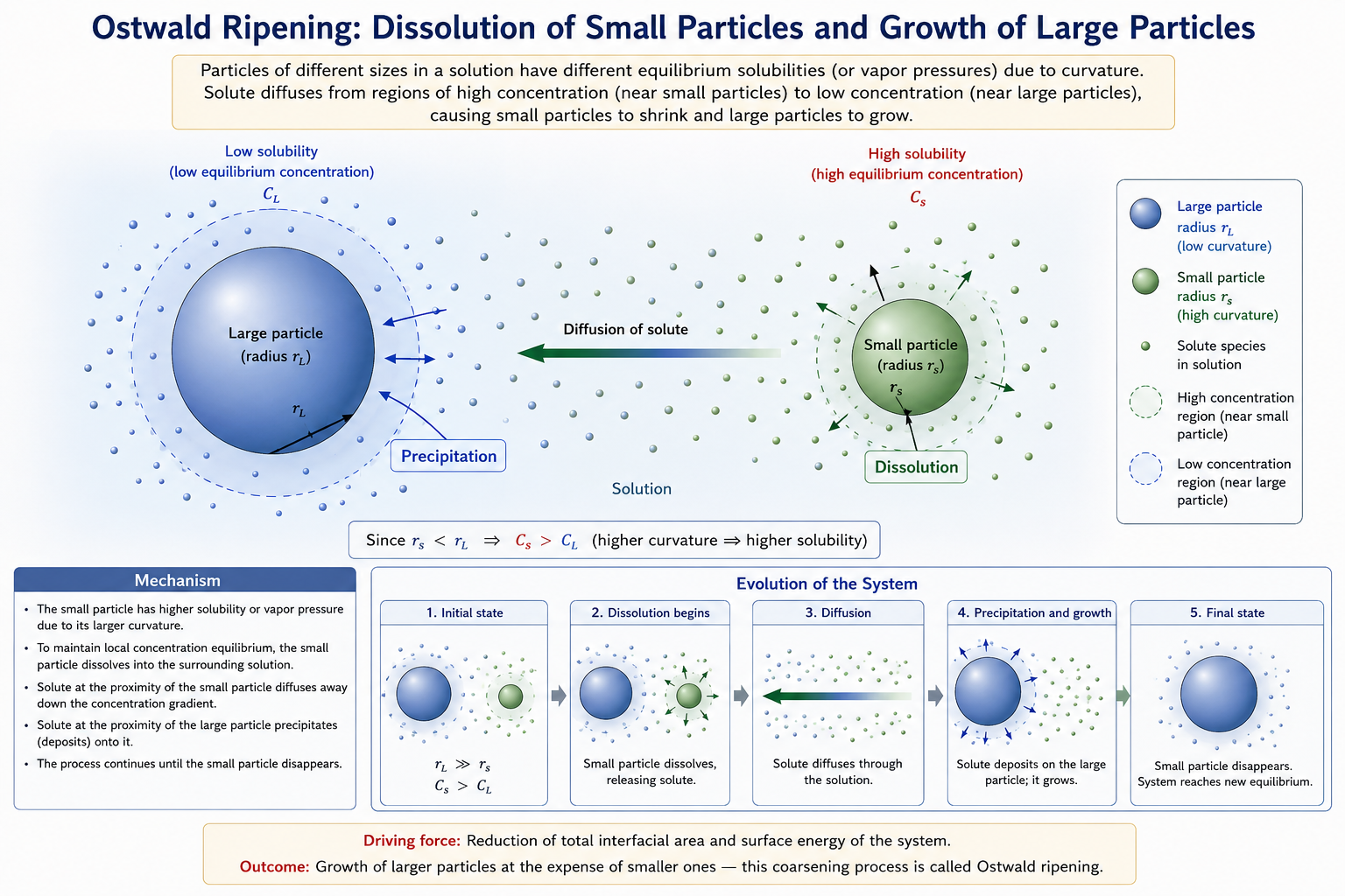
Fig. 6.5 Schematic of the Ostwald ripening process. The small particle (radius rs, right) has higher curvature and therefore higher equilibrium solubility — it dissolves into the surrounding solution. The dissolved solute diffuses through the solution (driven by the concentration gradient between the high-solubility small-particle region and the low-solubility large-particle region) and precipitates onto the large particle (radius rL, left). The process continues until the small particle disappears completely, reducing the total interfacial area and surface energy of the system.
The kinetics of Ostwald ripening follow the Lifshitz–Slyozov–Wagner (LSW) theory, which predicts that the mean particle radius ⟨r⟩ grows as ⟨r⟩³ ∝ t — that is, the cube of the mean radius increases linearly with time. This t1/3 growth law is a robust prediction that has been confirmed experimentally for a wide range of particle–solvent systems. It has important practical implications: even at low temperatures, given sufficient time, a nanoparticle dispersion will coarsen. The rate constant depends on the solubility S∞, the diffusion coefficient of the dissolved species, the surface energy γ, and temperature. High surface energy, high solubility, and high temperature all accelerate ripening.
Ostwald ripening is not always detrimental. It can be exploited deliberately to narrow the size distribution of a nanoparticle synthesis: if a polydisperse suspension is aged under controlled conditions, the smallest particles (the tail of the size distribution) dissolve preferentially, while the remaining particles grow more uniformly. This "digestive ripening" or "size-selective ripening" approach has been used to produce narrow size distributions of gold, silver, and semiconductor nanoparticles from initially broad distributions. However, in most practical applications — catalysis, drug delivery, quantum dot displays — Ostwald ripening is undesirable because it degrades the size-uniformity, surface area, and quantum-confinement properties that make nanomaterials valuable. Preventing it requires deliberate stabilisation strategies.
6 Stabilisation of Nanomaterials Against Coarsening
The thermodynamic driving force for surface energy reduction — whether through sintering, Ostwald ripening, or agglomeration — is always present in any nanoparticle system. Since this driving force cannot be eliminated (it is a fundamental consequence of the second law of thermodynamics applied to surfaces), the practical goal of nanomaterial synthesis and processing is to kinetically trap the nanostructure in a metastable state: to raise the activation energy for coarsening high enough that the desired nanoscale structure is preserved on practical timescales.
Several stabilisation strategies have been developed, each targeting a different aspect of the coarsening mechanisms:
- Steric stabilisation: coating nanoparticle surfaces with long-chain polymer or surfactant molecules creates a physical barrier that prevents particles from approaching closely enough to sinter or agglomerate. Polyethylene glycol (PEG), oleic acid, and block copolymers are widely used. The steric layer also reduces the solid–liquid interfacial energy, lowering the thermodynamic driving force for Ostwald ripening.
- Electrostatic stabilisation: charging nanoparticle surfaces (by adsorption of ions or through surface functional groups) creates a repulsive electrostatic double-layer that keeps particles separated. DLVO theory describes the balance between van der Waals attraction and electrostatic repulsion. Citrate-stabilised gold nanoparticles are a classic example — the negatively charged citrate anions electrostatically repel neighbouring particles.
- Capping agents and ligands: small organic molecules (thiols for gold, phosphines for semiconductor quantum dots, amines for metal oxides) bind strongly to specific crystal faces, reducing their surface energy and often providing steric protection simultaneously.
- Matrix encapsulation: embedding nanoparticles in a rigid solid matrix (silica, alumina, polymer, carbon) physically prevents particle contact and diffusion, suppressing both sintering and Ostwald ripening even at elevated temperatures. This approach is used in heterogeneous catalysts to maintain nanoparticle dispersion under reaction conditions.
- Grain boundary segregants: for bulk nanocrystalline metals, adding solute atoms that preferentially segregate to grain boundaries and reduce grain boundary energy (or mobility) dramatically retards grain growth. This is the basis of thermally stable nanocrystalline alloys designed for high-temperature structural applications.
The choice of stabilisation strategy depends on the application. For biomedical applications, biocompatible and biodegradable coatings (PEG, lipid shells) are essential. For heterogeneous catalysis, the stabiliser must not block the active surface sites. For electronic applications, the stabiliser must not impair charge transport between nanoparticles. In each case, the goal is the same: to preserve the nanoscale structure — and with it, the nanoscale properties — against the ever-present thermodynamic drive toward coarsening.
The importance of stabilisation cannot be overstated. It is not an afterthought of nanomaterial synthesis but an integral part of the design process. A nanoparticle that is perfectly synthesised but improperly stabilised will lose its nanoscale character — and its functional properties — within minutes, hours, or days. Conversely, a well-stabilised nanomaterial can maintain its structure for years, enabling the reliable and reproducible performance that practical applications demand.
Key Takeaways
- Any curved surface has two principal radii of curvature R1 and R2. The generalised Young–Laplace equation is Δμ = γΩ(1/R1 + 1/R2). Convex surfaces (positive curvature) raise chemical potential; concave surfaces lower it — driving mass flow from convex to concave regions.
- The Kelvin equation, ln(Pc/P∞) = 2γΩ/kRT, shows that vapour pressure above a small curved particle exceeds that above a flat surface — the smaller the particle, the higher the vapour pressure.
- The Gibbs–Thomson equation, ln(Sc/S∞) = γΩ(R1−1 + R2−1)/kT, is the solubility analogue: smaller particles are more soluble than larger ones.
- Ostwald ripening is driven by the solubility difference between small and large particles. Dissolved solute diffuses from the vicinity of small particles (high Sc) to large particles (low Sc), causing small particles to shrink and disappear while large particles grow. LSW theory predicts ⟨r⟩³ ∝ t.
- Ostwald ripening can be exploited to narrow particle size distributions, but is generally undesirable in applications requiring stable nanoscale structure.
- Nanomaterial stabilisation against coarsening is achieved by steric coating, electrostatic repulsion, capping ligands, matrix encapsulation, or grain boundary segregants — each raising the kinetic barrier to sintering, ripening, or agglomeration.
✦ References & Further Reading
- Cao, G. (2004). Nanostructures & Nanomaterials: Synthesis, Properties & Applications. Imperial College Press.
- Lifshitz, I. M. & Slyozov, V. V. (1961). The kinetics of precipitation from supersaturated solid solutions. J. Phys. Chem. Solids, 19(1–2), 35–50.
- Wagner, C. (1961). Theorie der Alterung von Niederschlägen durch Umlösen (Ostwald-Reifung). Z. Elektrochemie, 65, 581–591.
- Thomson, W. (Lord Kelvin) (1871). On the equilibrium of vapour at a curved surface of liquid. Phil. Mag., 42, 448–452.
- Ratke, L. & Voorhees, P. W. (2002). Growth and Coarsening: Ostwald Ripening in Material Processing. Springer.
- Israelachvili, J. N. (2011). Intermolecular and Surface Forces (3rd ed.). Academic Press.
Stabilization of Nanomaterials I
Electrostatic stabilization, the electrical double layer, and DLVO theory — the kinetic framework for preventing nanoparticle agglomeration in suspension.
Contents
1 Why Stabilization is Non-Negotiable
The reduction of overall surface energy is the thermodynamic driving force governing nanomaterial behaviour at every structural level. Left unchecked, this drive causes particles to agglomerate, fuse, or ripen — resulting in complete loss of the nanoscale functional properties that make these materials useful. Stabilization, both during synthesis and during storage and application, is therefore a mandatory processing step, not an optional refinement.
Two approaches are widely deployed. Electrostatic stabilization creates a repulsive energy barrier by establishing like charges on particle surfaces — it is a kinetic method. Steric stabilization coats surfaces with polymer chains that resist interpenetration — it is a thermodynamic method.
2 Origin of Surface Charge
When a solid particle emerges in a polar solvent or an electrolyte solution, a surface charge develops through one or more of the following mechanisms:
- Preferential adsorption of ions. Certain ions from solution are selectively taken up by the particle surface. For AgI particles in a solution containing Ag⁺ and I⁻, whichever ion is in excess is preferentially adsorbed, setting the sign of the surface charge.
- Dissociation of surface charged species. Surface functional groups ionize in solution (e.g. –COOH ⇌ –COO⁻ + H⁺). The degree of ionization is pH-dependent, making the surface charge tunable. This governs the behaviour of most oxide nanoparticles.
- Isomorphic substitution of ions. Lattice cations are replaced by lower-valence ions — for example Al³⁺ substituted by Mg²⁺ in a clay framework — creating a permanent structural charge independent of pH.
- Accumulation or depletion of electrons at the surface. In semiconductors and metals, charge redistribution arises from differences in Fermi levels or contact potentials at the surface.
- Physical adsorption of charged species onto the surface. Charged polyelectrolytes or surfactants adsorb onto the particle surface, transferring their charge character to it.
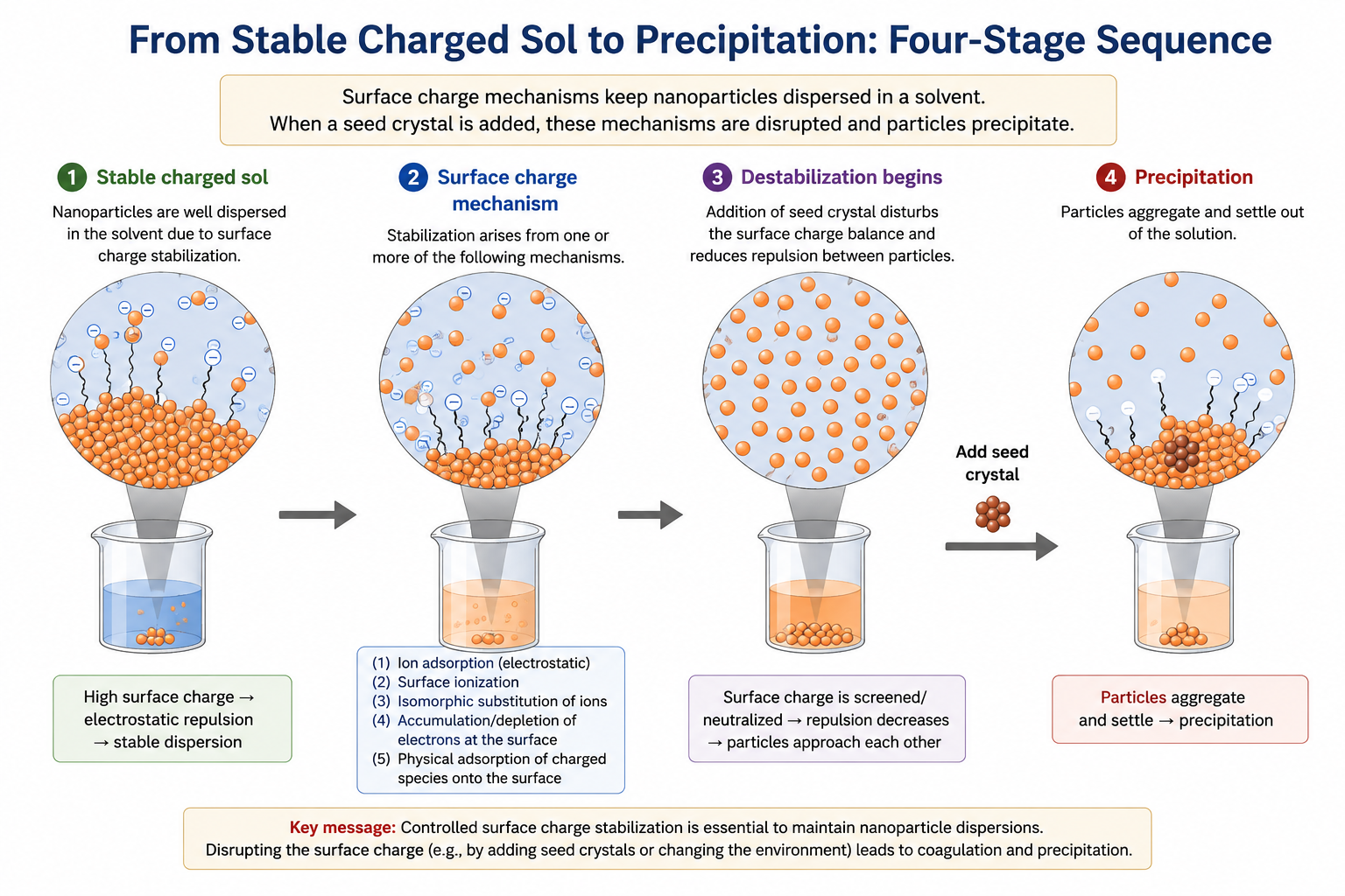
3 The Electrical Double Layer
Once a surface charge density is established, an electrostatic field segregates positive and negative species near the surface. This is opposed by two forces: Coulombic attraction pulling counter-ions toward the surface, and entropic dispersion and Brownian motion driving them back into the bulk. The resulting inhomogeneous ion distribution near the surface is the electrical double layer (EDL).
- Stern layer: extends from the solid surface to the Helmholtz plane. Counter-ions here are tightly bound and immobile. The electric potential drops linearly from the surface potential Φ₀ to the Stern potential Φ_H.
- Gouy (diffuse) layer: extends from the Helmholtz plane outward to the bulk. Ions are mobile; the potential decays exponentially.
- Zeta potential (Φ_z): the potential at the slip plane — the boundary between the fluid moving with the particle and the bulk solution. This is the experimentally measurable quantity; |ζ| > 30 mV typically indicates a stable suspension.
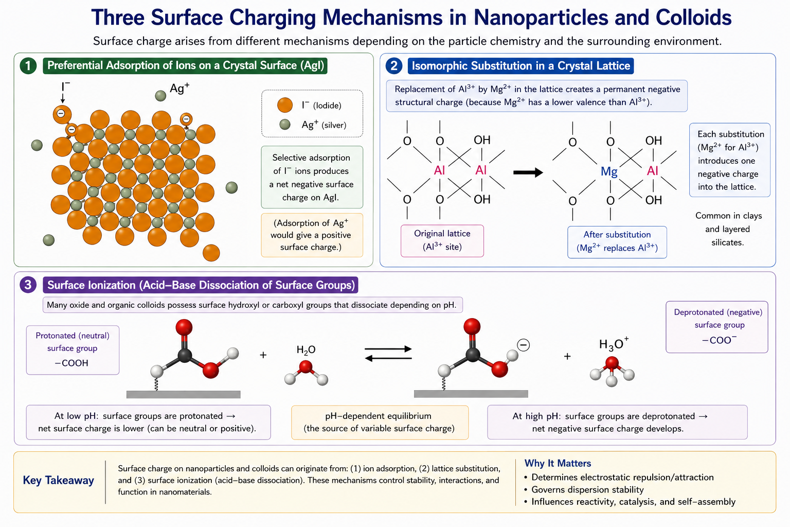
4 DLVO Theory
In a nanoparticle suspension, van der Waals forces and Brownian motion dominate while gravity is negligible. Van der Waals attraction is always present; Brownian motion ensures constant particle collisions. Without stabilization, the combined effect leads to agglomeration. The total interaction Φ between two electrostatically stabilized particles is given by DLVO theory (Derjaguin, Landau, Verwey, Overbeek):
where Φ_A is the attractive van der Waals potential and Φ_R is the repulsive electrostatic potential.
- Infinite flat surface; uniform surface charge density
- No redistribution of surface charge as particles approach
- No change in counter-ion concentration profiles on approach
- Solvent acts only via its dielectric constant; no chemical reactions between particle and solvent
- Dispersion is dilute; no external forces other than van der Waals and electrostatic
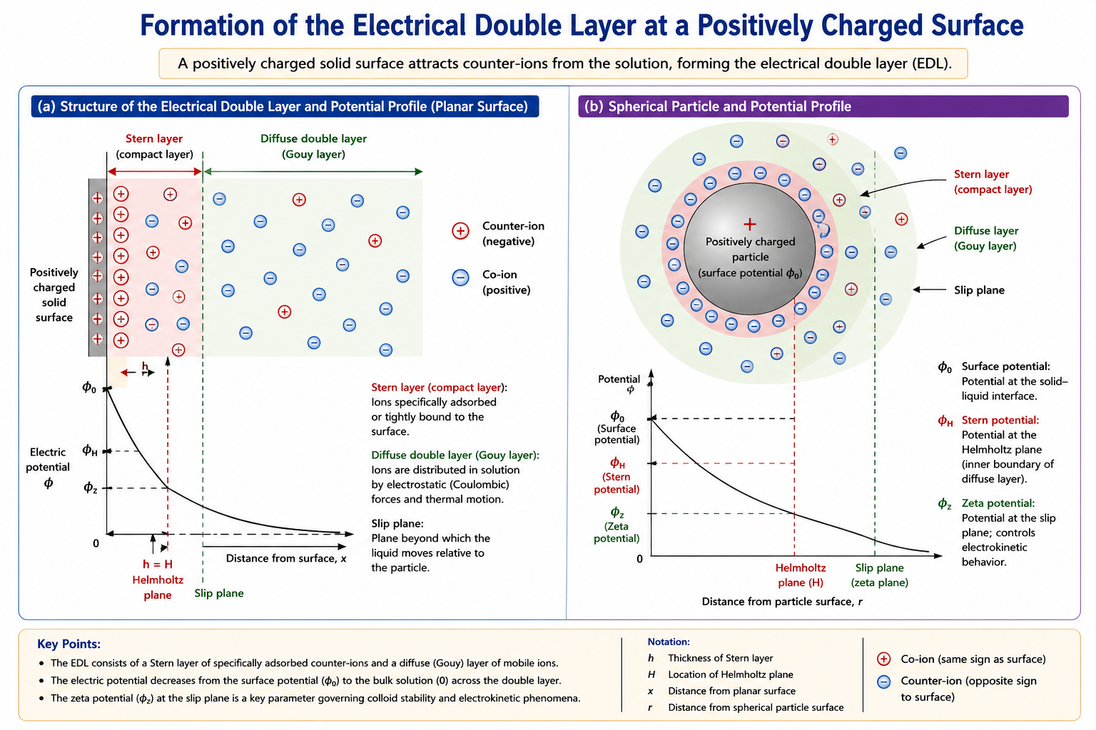
5 Effect of Double Layer Thickness
The stability barrier V_max depends critically on the Debye length κ⁻¹ (double layer thickness), which is set by the electrolyte concentration. Adding salt compresses the double layer, collapsing the barrier — the physical basis of salting out.
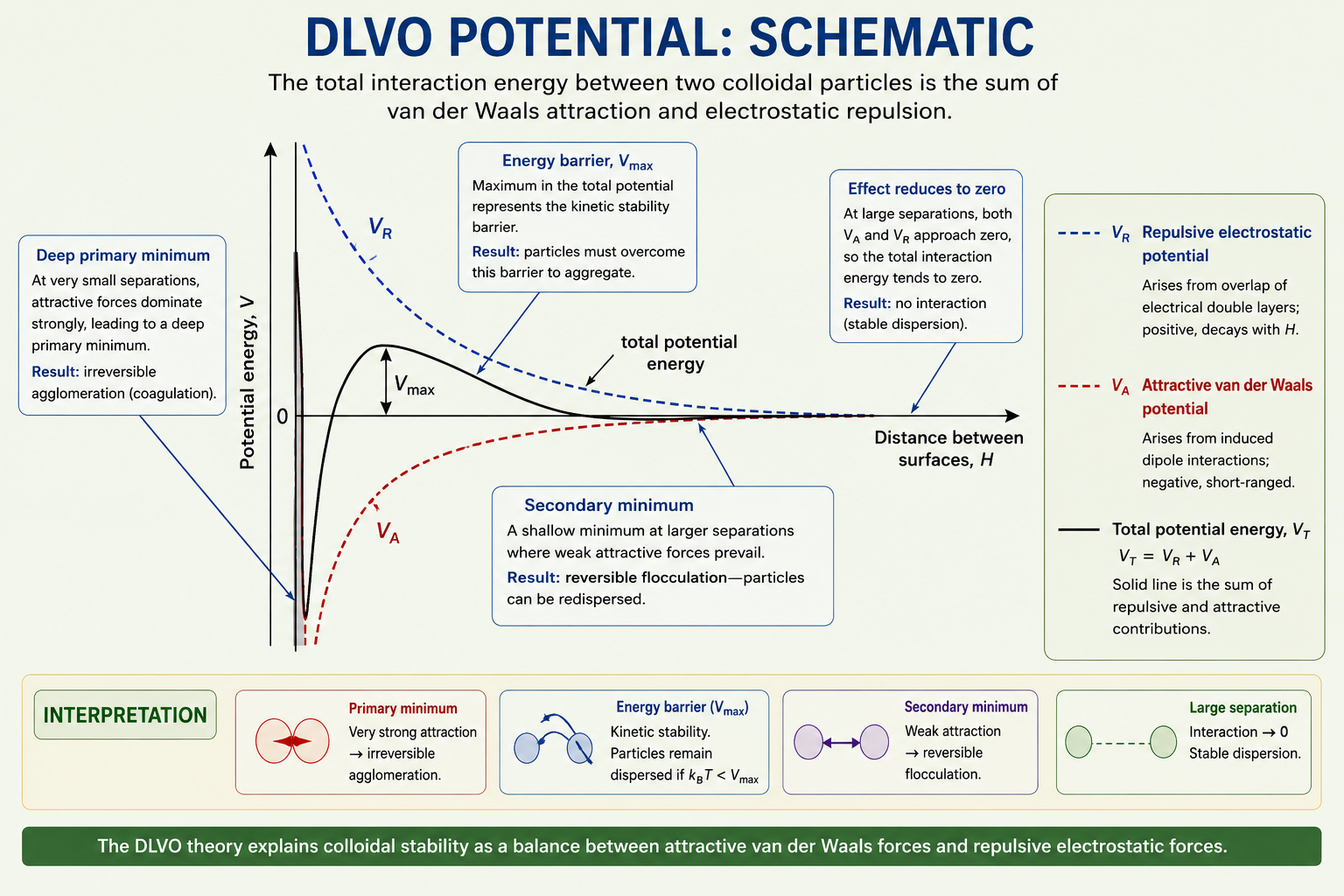
5b Effect of Double Layer Thickness on Stability
The stability barrier V_max depends on the Debye length κ⁻¹. Adding electrolyte compresses the double layer, collapsing the barrier — the physical basis of salting out.
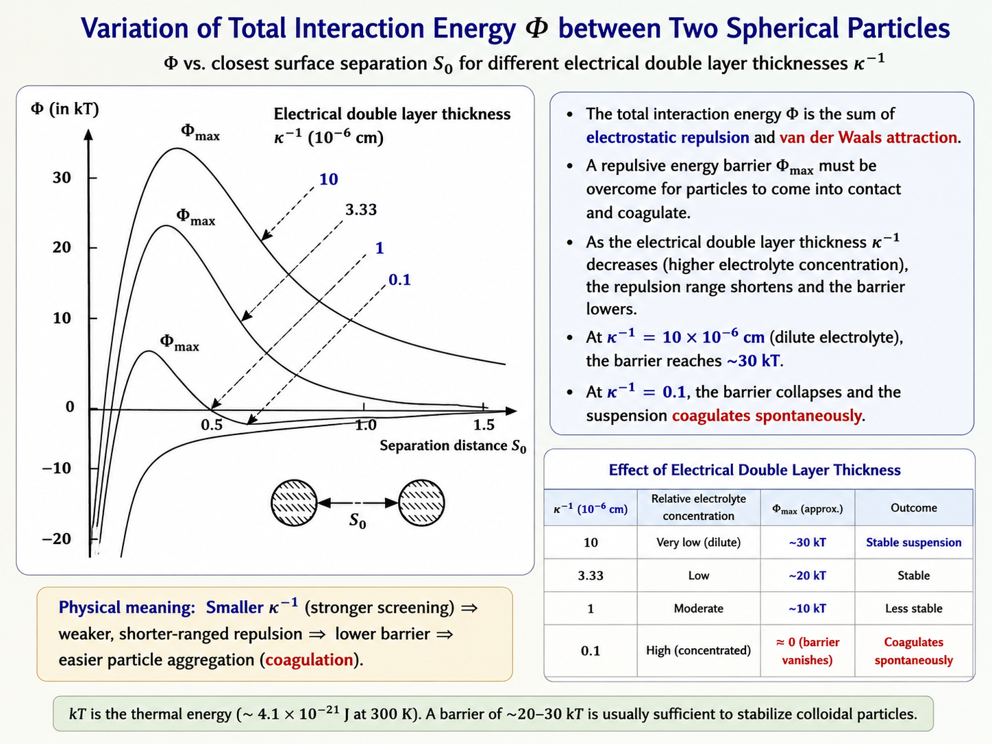
6 Conditions for Electrostatic Repulsion
Repulsion only acts when double layers overlap. When the surface separation S₀ exceeds 2d (twice the double layer thickness), there is no overlap and no repulsion. When S₀ < 2d, the double layers interpenetrate, generating an osmotic repulsive pressure.
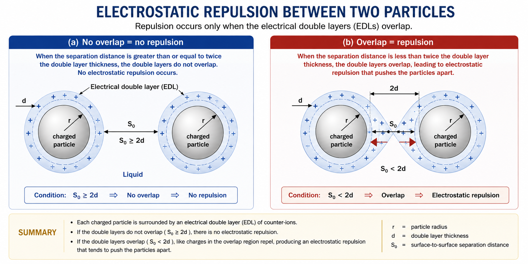
Key Takeaways
- Surface energy minimization drives agglomeration; stabilization is mandatory to preserve nanoscale properties.
- Surface charge arises from: preferential ion adsorption, surface group dissociation, isomorphic substitution, electron redistribution, physical adsorption of charged species.
- The EDL has two zones: Stern layer (linear potential drop, immobile ions) and Gouy layer (exponential decay, mobile ions). Zeta potential at the slip plane is the practical stability measure.
- DLVO: Φ = Φ_A + Φ_R. The energy barrier V_max prevents agglomeration when V_max ≫ k_BT.
- Adding electrolyte compresses the double layer (reduces κ⁻¹), lowers V_max, and eventually causes coagulation — the salting-out effect.
- Repulsion only acts when double layers overlap (S₀ < 2d).
✦ References & Further Reading
- Cao, G. (2004). Nanostructures & Nanomaterials: Synthesis, Properties & Applications. Imperial College Press.
- Israelachvili, J. N. (2011). Intermolecular and Surface Forces (3rd ed.). Academic Press.
- Derjaguin, B. & Landau, L. (1941). Theory of the stability of strongly charged lyophobic sols. Acta Physicochim. URSS, 14, 633–662.
- Verwey, E. J. W. & Overbeek, J. T. G. (1948). Theory of the Stability of Lyophobic Colloids. Elsevier.
Stabilization of Nanomaterials II
Limitations of electrostatic stabilization, steric (polymeric) stabilization, solvent quality, anchored vs. adsorbing polymers, and the thermodynamics of polymer layer interactions.
Contents
1 Validity and Limitations of Electrostatic Stabilization
DLVO theory remains valid only when the dispersion is sufficiently dilute (neighbouring double layers do not interfere), no other forces are significant (gravity negligible, no external fields), particle geometry is simple, and the double layer is purely diffusive (governed only by electrostatic, entropic, and Brownian forces). Outside these conditions the theory breaks down.
- Kinetic only: a kinetic barrier dependent on counter-ion concentration — any change in ionic strength can collapse it.
- Dilute systems only: breaks down at high particle concentrations.
- Electrolyte sensitive: fails in salt-rich media (physiological saline, seawater, industrial streams).
- Irreversible once agglomerated: particles reaching the primary minimum are practically impossible to redisperse.
- Unsuitable for multiple-phase systems: different solids carry different surface charges in a given condition, making simultaneous stabilization difficult.
2 Steric (Polymeric) Stabilization
Steric stabilization coats particle surfaces with polymer chains, creating a physical barrier against close approach. The mechanism is fundamentally thermodynamic — not merely kinetic.
- Thermodynamic: reversible — agglomerated particles can be redispersed by restoring solvent conditions.
- High concentration: effective even at high particle concentrations and in the absence of solvent.
- Not electrolyte sensitive: works equally in salt-free and salt-rich media.
- Multiple-phase systems: the same polymer can stabilize chemically different particles in a mixed suspension.
A further advantage relevant to synthesis: the polymer layer adsorbed on growing nanoparticles acts as a diffusion barrier for growth species, producing diffusion-limited growth. This reduces the spread in particle size, yielding monosized nanoparticles. The polymer simultaneously provides colloidal stability and controls particle size during synthesis.
The molecular mechanism of steric stabilization can be understood in terms of osmotic pressure. Polymer chains grafted or adsorbed onto a particle surface extend into the surrounding solvent, forming a diffuse corona. When two polymer-coated particles approach each other and the surface separation falls below twice the polymer layer thickness, the polymer coronas begin to overlap. In this overlap zone, the local polymer segment concentration increases sharply above that of the surrounding bulk solution. This concentration gradient creates an osmotic pressure difference that drives solvent molecules into the gap between the particles, effectively pushing them apart. The osmotic repulsion scales with the polymer concentration in the overlap region and with the quality of the solvent — in a good solvent, the polymer-solvent interaction is enthalpically favourable, and the system strongly resists any increase in local polymer concentration. This osmotic contribution, combined with the entropic penalty of restricting polymer chain conformations upon compression, produces a robust repulsive barrier that keeps particles well-dispersed.
3 Solvent Quality and the Theta Temperature
- Good solvent: polymer tends to expand, reducing the overall Gibbs free energy — polymer–solvent interactions are favourable. Provides a thick, effective steric barrier.
- Poor solvent: polymer tends to collapse (coil), preferring polymer–polymer contacts. A collapsed layer offers little steric protection.
- Temperature dependence: solvent quality changes with temperature — polymer expands at high T, collapses at low T (for most systems).
- Theta temperature (θ): the temperature at which the transition from good to poor solvent occurs. At T = θ, ΔG = 0 for chain expansion or collapse. Below θ, the polymer collapses and stabilization fails.
The solvent quality for a given polymer-solvent pair is quantified by the Flory-Huggins interaction parameter χ (chi). This dimensionless parameter captures the net enthalpic cost of placing a polymer segment in solvent rather than among other polymer segments. When χ < 0.5, the polymer-solvent contacts are energetically favourable and the polymer chain swells — this defines a good solvent. At χ = 0.5, the enthalpic mixing penalty exactly cancels the excluded-volume expansion of the chain, and the polymer adopts its unperturbed random-walk conformation — this is the theta (θ) condition, and the corresponding temperature is the theta temperature. When χ > 0.5, polymer-polymer contacts become more favourable than polymer-solvent contacts, causing the chain to collapse into a compact globule — a poor solvent. At the theta temperature, the second virial coefficient of the polymer solution vanishes, meaning that the excluded volume effects arising from monomer-monomer repulsion exactly cancel the attractive interactions between chain segments. For steric stabilization, one must operate well above the theta temperature (χ well below 0.5) to ensure that the polymer chains remain fully extended and provide a thick, effective barrier against particle aggregation.
4 Types of Polymer Attachment
Polymers attach to solid surfaces in three configurations. The interaction between polymer and solid surface is governed by weak physical forces only — chemical reactions or further polymerization between polymer and solvent or between polymers are not considered.
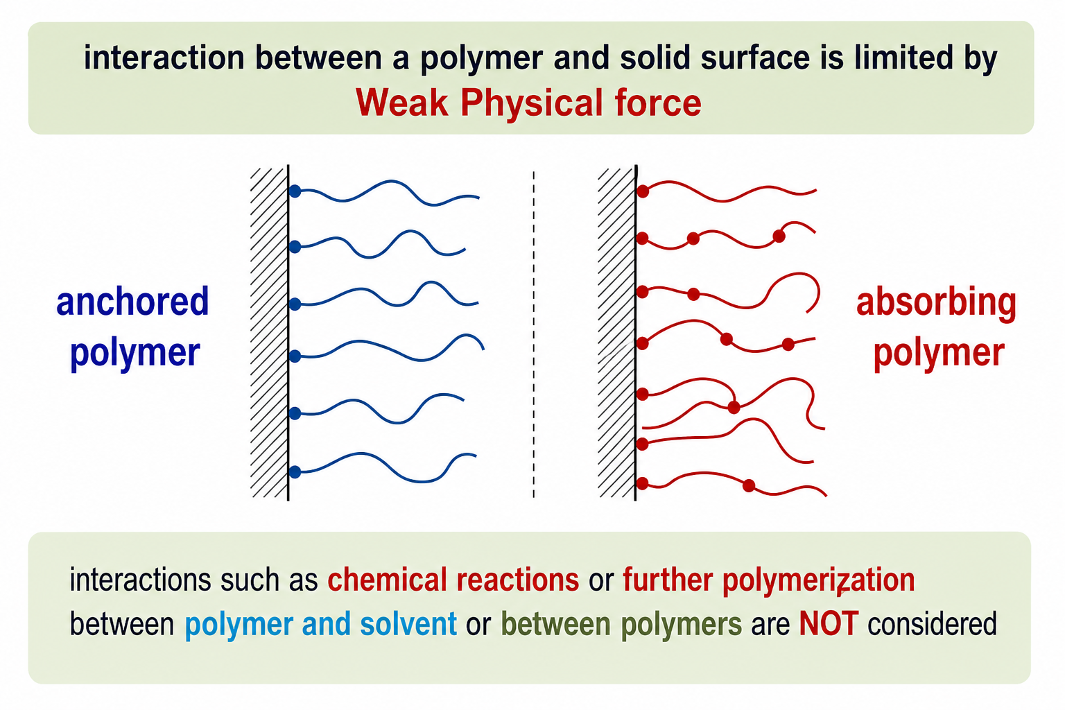
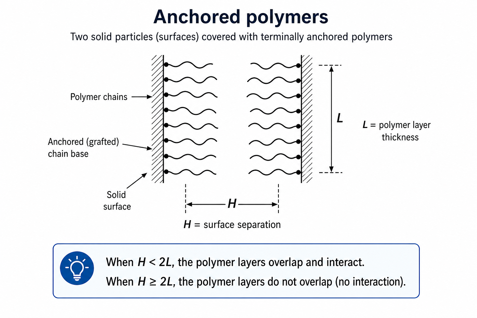
5 Steric Repulsion: Anchored Polymers in a Good Solvent
In a good solvent, in which polymer expands, if the coverage of polymer on the solid surface is not complete (particularly less than 50%), insufficient polymer concentration means two polymer layers tend to interpenetrate to reduce available space between them. Such interpenetration reduces the freedom of the polymer chains, decreasing entropy. Since ΔH ≈ 0 in a good solvent, ΔG = ΔH − TΔS > 0 — the interpenetration is thermodynamically unfavourable and generates a repulsive force.
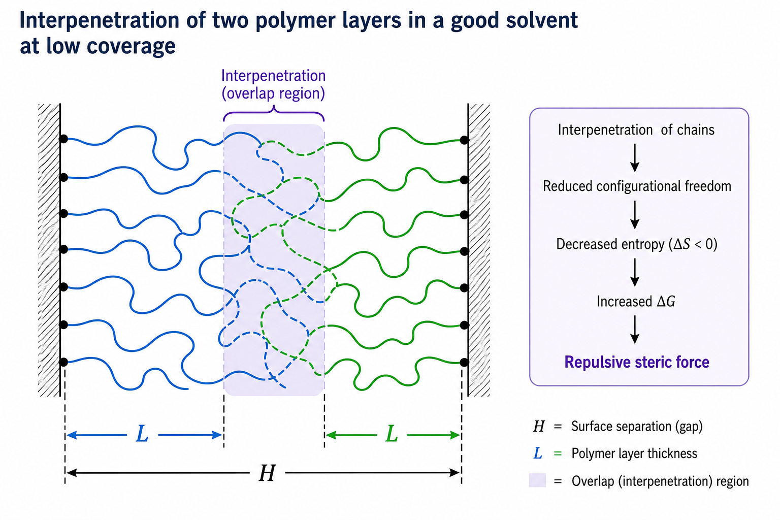
When coverage is high (approaching 100%), there is no interpenetration. Instead, as the two surfaces approach, the polymer layers are compressed — polymers coil up in both layers. This compression raises the free energy steeply at separations below 2L.
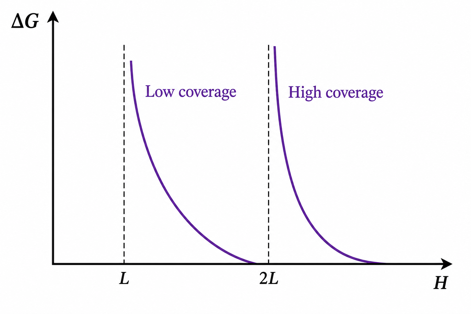
6 Anchored Polymers in a Poor Solvent
In a poor solvent with low coverage, the surface of one particle tends to penetrate into the polymer layer of the approaching particle. Such interpenetration promotes further coiling of the polymers, reducing the overall Gibbs free energy — the interaction is attractive and promotes agglomeration.
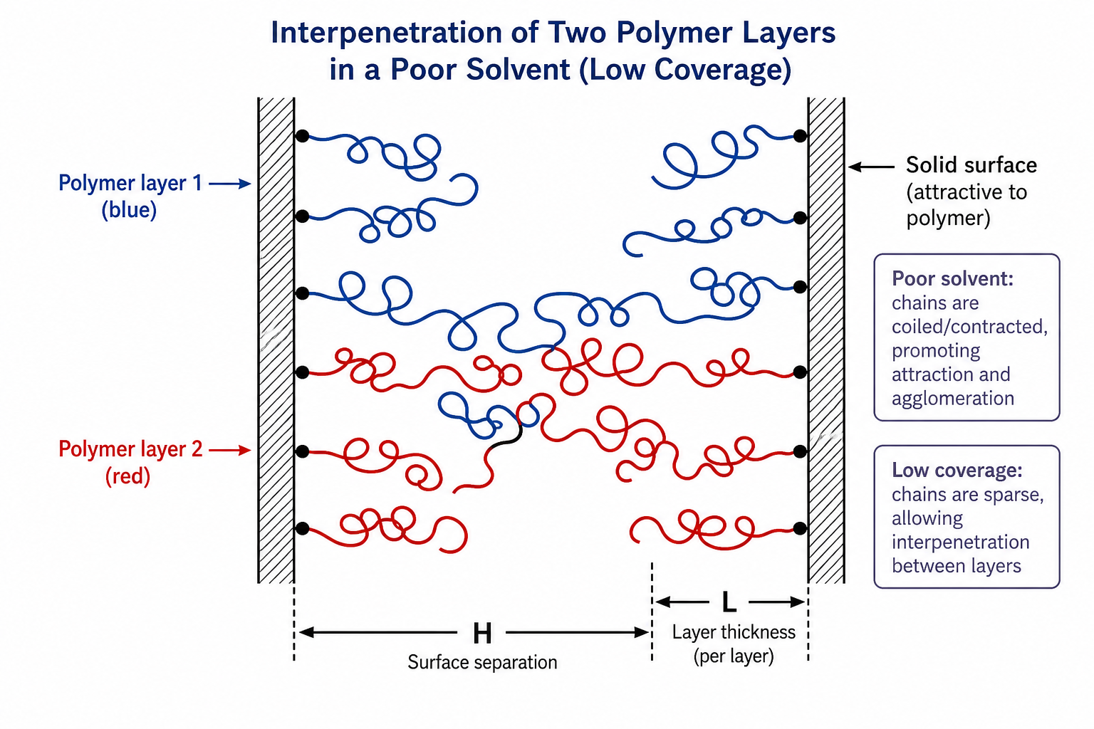
With high coverage in a poor solvent, similar to the good solvent case, there is no penetration. The reduction in distance results in a compressive force, leading to an increase in overall free energy — giving repulsion.
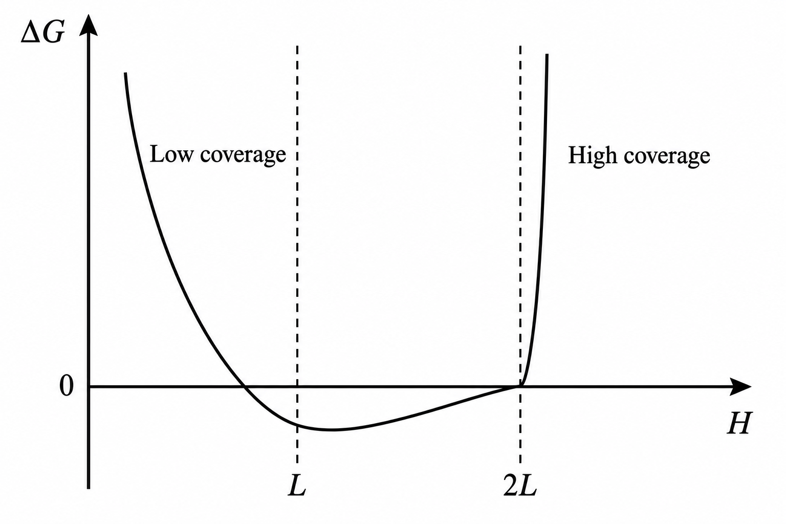
Regardless of differences in coverage and solvent quality, two particles covered with sufficient polymer layers are prevented from agglomeration by the combination of space exclusion (steric effect) and the thermodynamic penalty of polymer layer compression. Use a good solvent (or operate above θ), achieve high surface coverage (~100%), use polymers of sufficient chain length, and prefer terminally anchored polymers where possible.
In practice, the most robust stabilization strategy is electrosteric stabilization, which combines both electrostatic and steric mechanisms simultaneously. This is achieved by using polyelectrolytes — polymers that carry ionisable groups along their backbone or side chains — as the stabilizing agent. When adsorbed or grafted onto a particle surface, polyelectrolytes provide a steric polymer barrier while also imparting a surface charge that generates an electrostatic double-layer repulsion. The two mechanisms act cooperatively: the electrostatic component provides a long-range repulsive barrier that keeps particles separated at large distances, while the steric component provides a strong short-range barrier that prevents close approach even if the electrostatic repulsion is partially screened by electrolyte. This dual protection makes electrosteric stabilization far more tolerant of changes in ionic strength, pH, and temperature than either mechanism alone. Many commercial nanomaterial dispersions — including those used in coatings, inks, biomedical imaging agents, and drug delivery vehicles — rely on electrosteric stabilization using polyelectrolytes such as poly(acrylic acid), poly(styrene sulfonate), or chitosan to maintain long-term colloidal stability under a wide range of processing and application conditions.
Key Takeaways
- Electrostatic stabilization is kinetic, electrolyte-sensitive, limited to dilute systems, and irreversible on agglomeration.
- Steric stabilization is thermodynamic, electrolyte-insensitive, reversible, and works at high concentration — more robust for practical applications.
- Polymer layers also act as diffusion barriers during synthesis, narrowing particle size distributions toward monosized.
- Good solvent → expanded chain → thick effective barrier. Poor solvent → collapsed chain → reduced protection.
- Theta temperature θ marks the good-to-poor solvent transition. Stabilization fails below θ for most systems.
- Good solvent, any coverage → repulsive. Poor solvent, low coverage → attractive (promotes agglomeration). Poor solvent, high coverage → repulsive.
✦ References & Further Reading
- Cao, G. (2004). Nanostructures & Nanomaterials: Synthesis, Properties & Applications. Imperial College Press.
- Napper, D. H. (1983). Polymeric Stabilization of Colloidal Dispersions. Academic Press.
- Fleer, G. J. et al. (1993). Polymers at Interfaces. Springer.
Adsorbing Polymers & 0-D Nanomaterials
Adsorbing polymer stabilization, physical basis of steric repulsion, and synthesis methods for 0-D nanoparticles — inert-gas condensation, free-jet expansion, and sonochemical processing.
Contents
1 Adsorbing Polymers
Adsorbing polymers — attaching via multiple random contact points along the backbone — are more complex than anchored polymers for two reasons:
- Bridging flocculation: a polymer chain on one particle may adsorb onto a second approaching particle, forming a physical bridge that attracts rather than repels them. Most likely at low surface coverage when unoccupied sites are abundant on both particles.
- Desorption and migration: adsorbed chains can desorb and migrate out of the layer over time, depleting the protective coating and reducing long-term stability — a limitation not shared by permanently anchored polymers.
2 Steric Interactions with Adsorbing Polymers
Two partially covered surfaces approaching in a good solvent: layers interpenetrate, reducing available space and forcing more ordered polymer arrangement. Entropy decreases, free energy increases — a repulsive interaction results when separation falls below twice the polymer layer thickness.
With strong adsorption and full coverage, the interaction is purely repulsive — ΔG increases as separation falls below twice the layer thickness, through a pure compression mechanism identical to anchored high-coverage case.
Interpenetration promotes further coiling, increasing chain entropy (collapsed state favoured) and reducing free energy at intermediate separations — producing an attractive interaction. However, at separations below the polymer layer thickness, a compressive repulsive force still develops, pushing the particles apart.
In all cases of sufficient coverage, the repulsive force that develops as particles approach within twice the polymer layer thickness prevents agglomeration — regardless of solvent quality.
3 Physical Basis of Steric Stabilization
- Volume restriction (entropic) effect: as two polymer-coated surfaces approach, polymer chains in the gap lose configurational freedom — fewer conformations are accessible. ΔS < 0, so ΔG = −TΔS > 0 at constant T. This entropy-driven repulsion is the dominant mechanism for anchored polymers in good solvents.
- Osmotic (concentration) effect: as particles approach, polymer segment concentration in the gap rises above its equilibrium value. Solvent diffuses in to dilute it (osmotic pressure), pushing the particles apart.
Carboxyl (–COOH), hydroxyl (–OH), amine (–NH₂), and ester (–COO–) groups in the polymer structure play key roles. Widely used stabilizers:
- PVP (Poly(vinylpyrrolidone)) — noble metal nanoparticles (Ag, Au, Pt)
- PVA (Polyvinylalcohol) — water-soluble, biocompatible
- Polyethyleneimine — cationic, oxide nanoparticles
- Sodium polyacrylate — anionic, dual electrostatic + steric
- Tetraalkylammonium halogenides — metal nanoparticles
4 Synthesis Methods for 0-D Nanomaterials
Having established how to stabilize nanoparticles once formed, the course now addresses how they are made. Synthesis methods are classified by the dimensionality of the nanostructure produced and by the class of nanostructure. The focus is 0-D Class 1 — discrete nanoparticles with all three dimensions at the nanoscale.
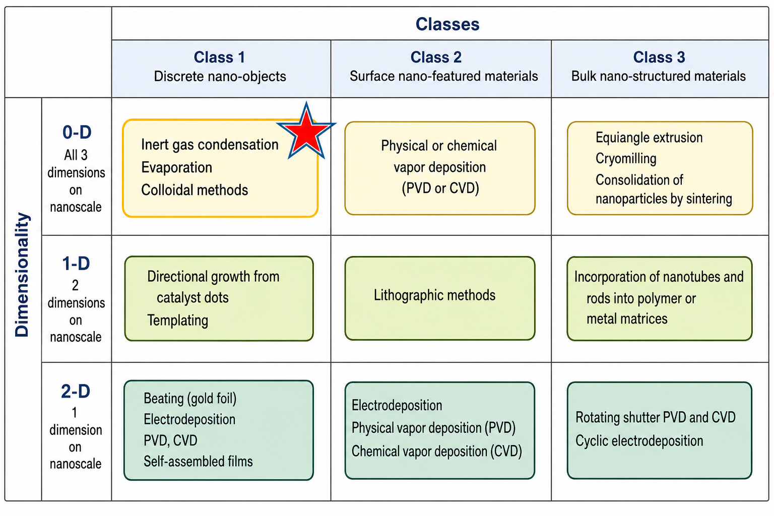
5 Method 1: Inert-Gas Condensation
The most established physical method for producing discrete nanoparticles from inorganic materials with low melting points (Al, Zn, Mg, noble metals). The process occurs in a vacuum chamber backfilled with He or Ar at low pressure:
- Source material evaporated from one or two evaporation sources (dual sources for alloy nanoparticles).
- Evaporated atoms rapidly lose energy by colliding with the inert gas atoms — rapid thermal moderation.
- Vapour supersaturates, nucleates, and forms clusters/nanoparticles (1–100 nm).
- Particles migrate thermophoretically upward and deposit on the cold finger (liquid-N₂ cooled surface).
- Harvested by scraping under inert atmosphere.
Key challenge: cluster formation — particles tend to aggregate on the cold finger.
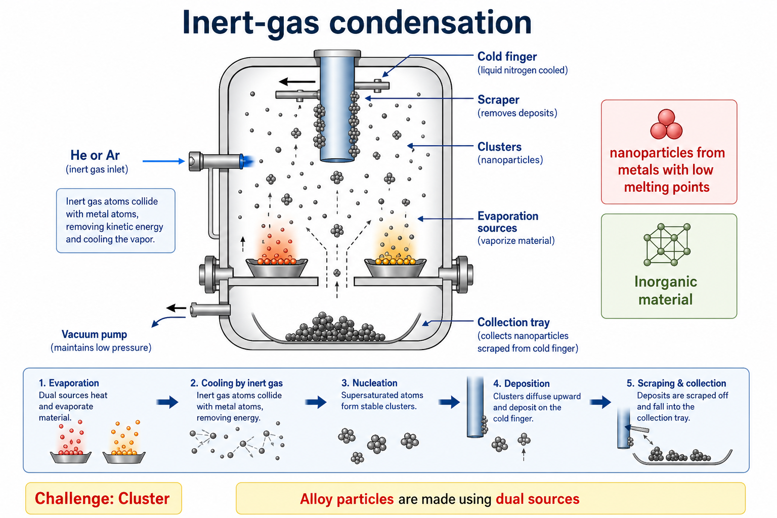
6 Method 2: Inert-Gas Free-Jet Expansion
A variant achieving faster, more controllable cooling. Evaporated atoms are carried by a high-pressure helium gas stream and expanded through a nozzle into a low-pressure chamber. The adiabatic free-jet expansion causes sudden rapid cooling, forcing nucleation of clusters. Key challenge: cluster size and distribution.
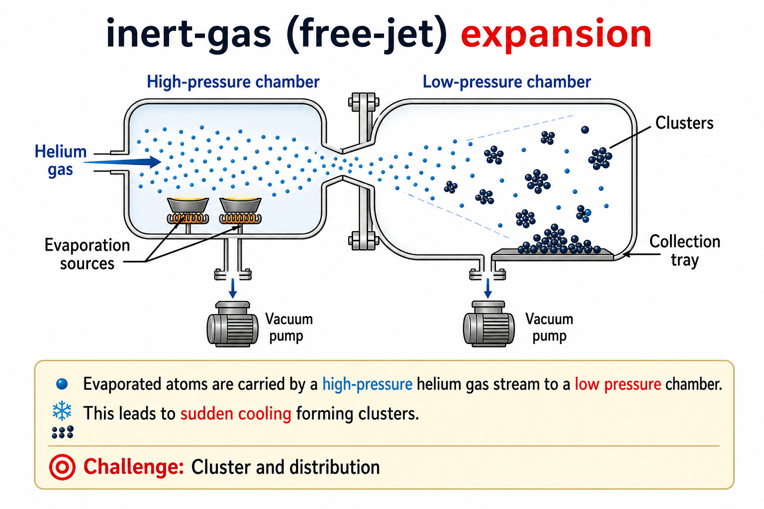
7 Method 3: Sonochemical Processing
Ultrasound (15 kHz to 1 GHz) is used to nucleate a chemical reaction. Acoustic cavitation produces alternating compression and tension cycles in the liquid, nucleating microscopic bubbles that grow then collapse violently. The collapse is adiabatic, generating transient temperatures ~5,000 K and pressures ~500 atm in the reacting hotspots, decomposing precursors and nucleating nanoparticles.
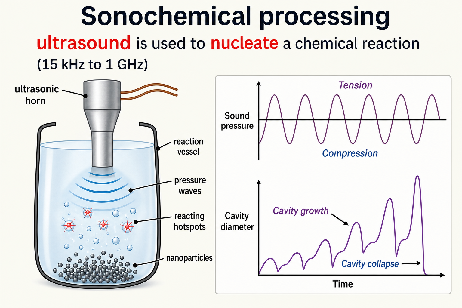
Key Takeaways
- Adsorbing polymers introduce bridging flocculation and desorption risks not present with anchored polymers.
- Steric repulsion has two physical origins: volume restriction (entropic — loss of chain conformations) and osmotic effect (solvent driven into the gap by elevated polymer concentration).
- Common stabilizers: PVP, PVA, polyethyleneimine, sodium polyacrylate, tetraalkylammonium halogenides.
- 0-D Class 1 nanoparticles are synthesized by: inert-gas condensation (evaporate → cool by gas collisions → deposit on cold finger → scrape; challenge: clusters), free-jet expansion (evaporate → sweep with high-pressure He → expand into low-pressure chamber → sudden cooling; challenge: size distribution), and sonochemical processing (ultrasound → cavitation → extreme T & P at hotspots → nanoparticle nucleation).
✦ References & Further Reading
- Cao, G. (2004). Nanostructures & Nanomaterials: Synthesis, Properties & Applications. Imperial College Press.
- Suslick, K. S. (1990). Sonochemistry. Science, 247(4949), 1439–1445.
- Gleiter, H. (2000). Nanostructured materials: basic concepts and microstructure. Acta Materialia, 48(1), 1–30.
Synthesis Methods for 0-D Nanostructures
Sonochemical processing, sol-gel synthesis, milling and attrition, repeated thermal cycling, and micelle-based self-assembly for nanoparticle production.
Contents
1 Sonochemical Processing
In sonochemical processing, ultrasound (15 kHz to 1 GHz) is used to nucleate a chemical reaction. Ultrasonic waves are transmitted through a reaction vessel via a transducer horn, generating acoustic pressure waves in the liquid. Because the acoustic wavelength (1–10,000 µm) is far above molecular dimensions, there is no direct coupling to chemical species — instead, reaction occurs at sites of cavitation.
Cavitation occurs when the tensile part of the pressure wave pulls the liquid apart, forming a tiny cavity. The compression part then collapses this bubble. When a bubble reaches a critical size the collapse is so fast that the process is effectively adiabatic, creating extreme local "hot spots" with temperatures ~5,000 °C and pressures of thousands of atmospheres — enough to trigger nanoparticle formation.
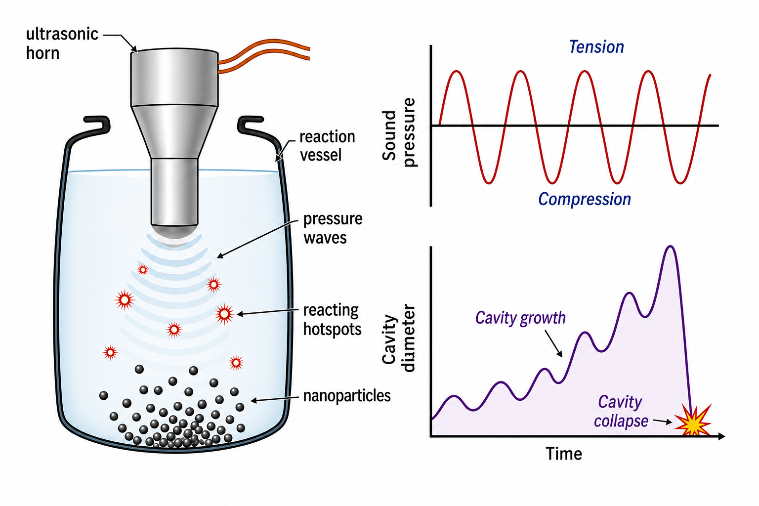
Using organometallic precursors — such as tetra-ethyl nickel, diethylmagnesium, and diethylzinc — oxide, carbide, and metallic nanoparticles can be synthesised. The size of the cavitation hotspot determines the size of the resulting nanoparticle.
2 Sol-Gel Process
The sol-gel process produces ultrafine particles, nanoscale films, and nanoporous membranes. The starting point is a solution of a metal alkoxide precursor (e.g. Ti(OC₄H₉)₄) in a suitable solvent. Adding a surfactant initiates polymerisation, forming a colloidal suspension called the sol. This can be processed in several ways:
- Into discrete nanoparticles or thin film coatings
- Reacted with a chemical agent to form a cross-linked 3D or 2D network — the "gel"
- Evaporation of solvent to form a nanoporous film
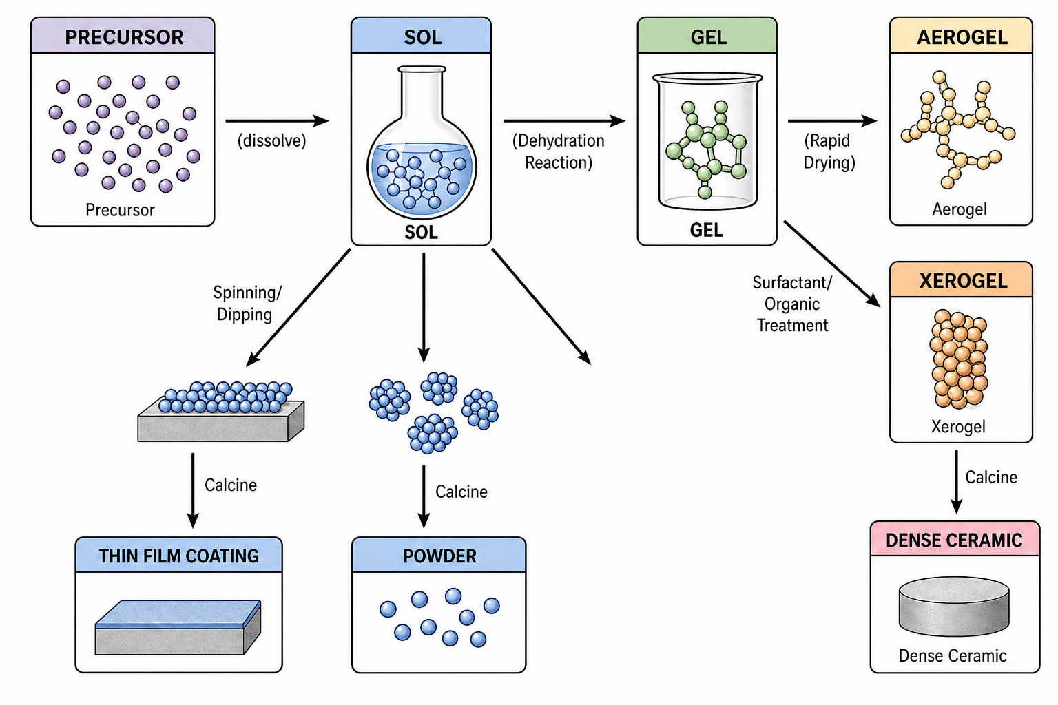
Mechanism of Sol-Gel Formation
Three sequential steps drive the process:
- Partial hydrolysis of metal alkoxides → reactive monomers
- Condensation of monomers → colloid-like oligomers (few repeating units) = sol formation
- Additional hydrolysis → cross-linking and polymerisation → three-dimensional network = gel formation
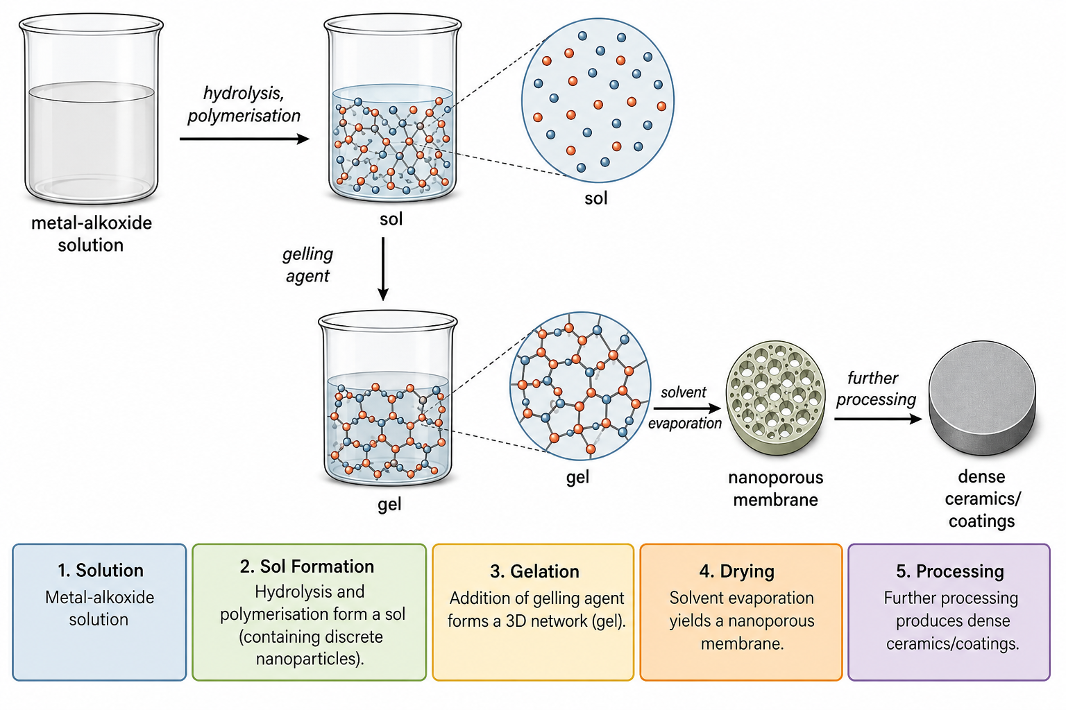
3 Milling and Attrition
Milling and attrition are classic top-down approaches. Ball mills and attritors use refractory or steel balls in an inert atmosphere to mechanically break bulk material down to nanoscale grain sizes.
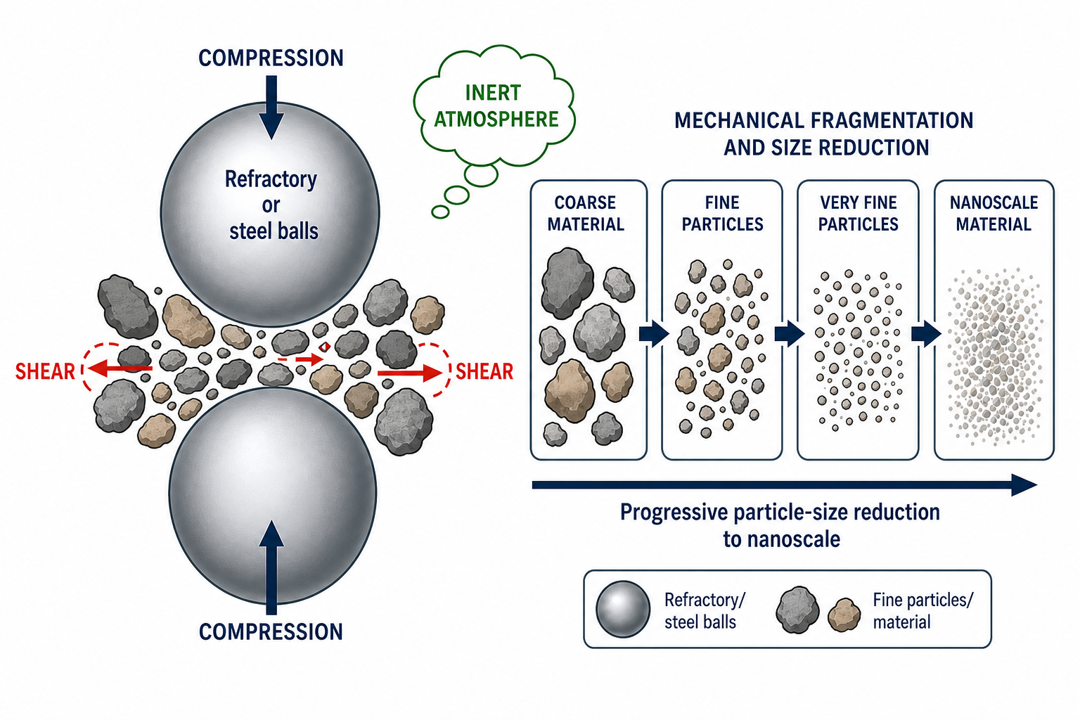
Limitations: broad size distribution, varied particle shape, impurities from the milling medium, and crystal defects — not ideal for device/functional applications.
Best suited for: nanocomposites and nano-grained bulk structural materials, where broad size distributions and small impurity levels are acceptable. Defects can often be annealed out during sintering.
4 Repeated Thermal Cycling
Repeated thermal cycling (quenching) can fracture bulk ceramic materials by exploiting two properties: very low thermal conductivity and large volume change with temperature. A phase transition accompanied by a large volume change is particularly effective. Limitations: only applicable to materials with poor conductivity but large volume change; particle size is hard to control precisely.
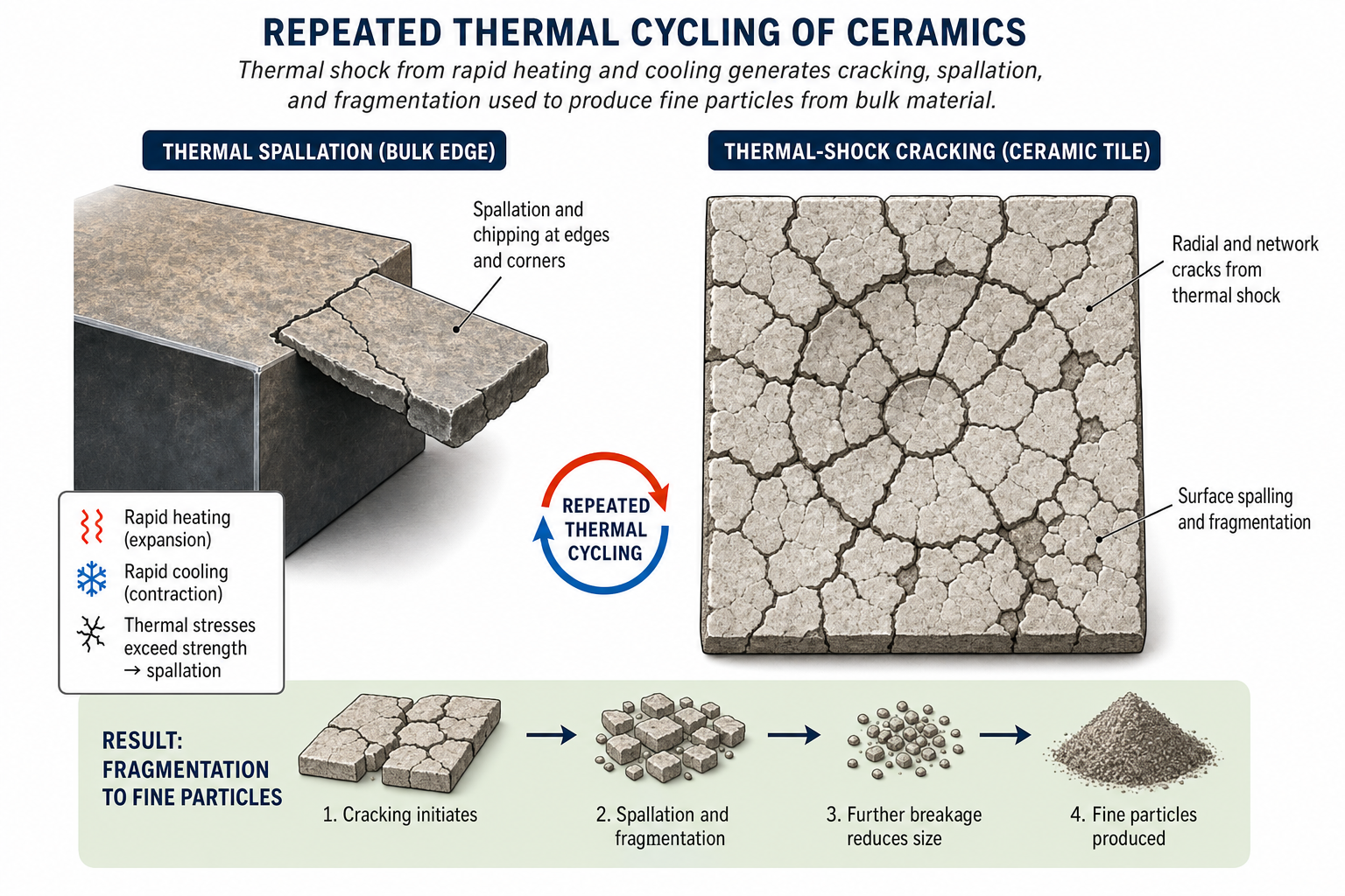
5 Micelle Synthesis — Molecular Self-Assembly
Nanoparticles can be synthesised by confining chemical reactions within a very small space, such as the core of a micelle. Micelles (microemulsions) are aggregates of amphiphilic molecules — one end soluble in water, the other end repelling water — that form spontaneously above a critical concentration. The centre of the micelle acts as a nanoscale reaction chamber, dictating the size of the nanoparticles created.
This is a classic example of molecular self-assembly: methods that rely on the self-organisation of organic molecules. In fact, the whole of the natural world is self-assembled.
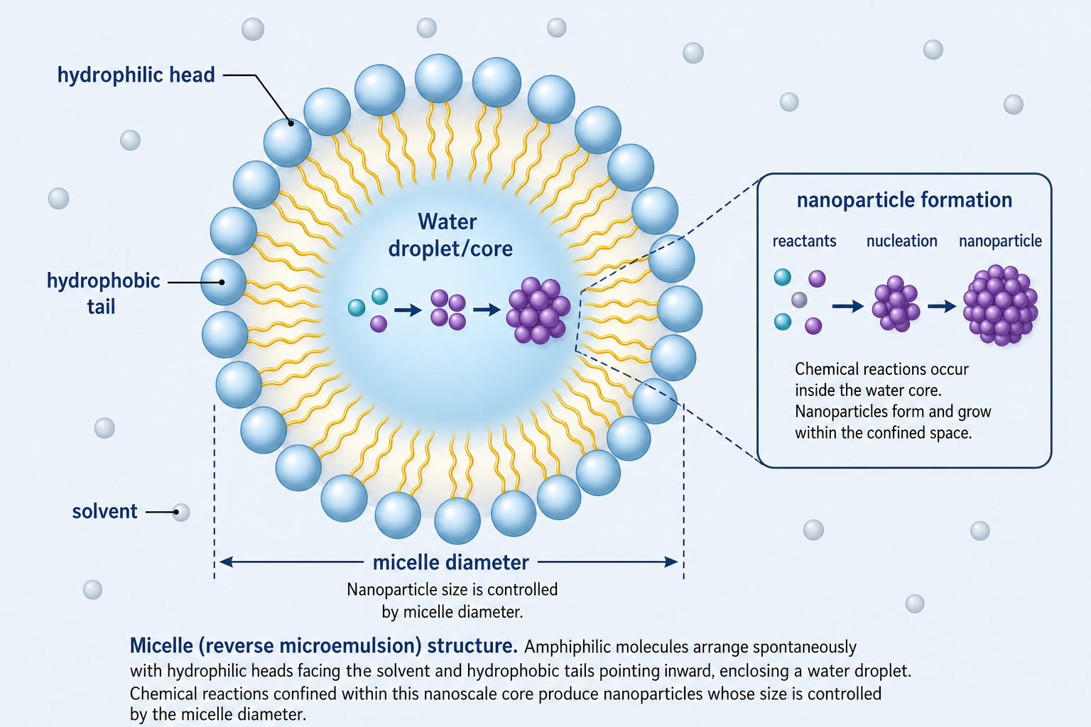
Nanoparticle synthesis methods fall into two broad categories. Thermodynamic approach: (i) generate supersaturation, (ii) nucleate, (iii) grow. Kinetic approach: control particle size by limiting the amount of precursor available or confining the reaction space (as in micelle synthesis).
In the thermodynamic approach, the formation of a spherical nucleus of radius r involves a competition between two energy contributions. The volume free energy term, -(4/3)πr³ΔGv, is negative and drives nucleation because the new phase is more stable than the supersaturated parent phase. The surface energy term, +4πr²γ, is positive and opposes nucleation because creating a new interface costs energy. The total free energy change is therefore ΔGtotal = -(4/3)πr³ΔGv + 4πr²γ. Setting the derivative d(ΔG)/dr = 0 to find the maximum gives -4πr²ΔGv + 8πrγ = 0, which yields the critical radius r* = 2γ/ΔGv. Substituting r* back into the total free energy expression gives the critical free energy barrier ΔG* = 16πγ³/(3ΔGv²). This barrier represents the activation energy that must be overcome for a stable nucleus to form. Nuclei smaller than r* are unstable and dissolve back into solution, while nuclei larger than r* are stable and grow spontaneously. The key insight is that both r* and ΔG* decrease with increasing supersaturation (larger ΔGv), making nucleation progressively easier as the system is driven further from equilibrium.
The nucleation rate — the number of stable nuclei formed per unit volume per unit time — follows an Arrhenius-type relationship: J = A·exp(-ΔG*/kBT), where A is a pre-exponential factor related to the frequency of atomic attachment and kBT is the thermal energy. Because ΔG* appears in the exponent, the nucleation rate is extraordinarily sensitive to the degree of supersaturation. Below a critical supersaturation level, ΔG* is so large that the exponential term is vanishingly small and nucleation is effectively negligible — the solution remains metastable. As supersaturation increases and ΔG* decreases, there is a narrow concentration window over which the nucleation rate increases by many orders of magnitude, producing burst nucleation — a sudden, explosive formation of a large number of nuclei in a very short time. This extreme sensitivity is the physical basis of LaMer's model of monodisperse particle formation, which exploits the sharp nucleation threshold to separate the nucleation and growth stages in time.
The practical implication for nanoparticle synthesis is that achieving monodisperse particles requires all nuclei to form at essentially the same moment, so that every particle subsequently experiences identical growth conditions. This is accomplished by rapidly injecting precursors (the "hot injection" technique) to drive the solution concentration above the critical supersaturation threshold as quickly as possible, triggering a single burst of nucleation. The burst consumes precursor and drops the concentration below the nucleation threshold, after which only slow, diffusion-controlled growth proceeds. Because no new nuclei form during the growth stage, all particles grow from the same starting size under the same conditions, producing a narrow size distribution. If, by contrast, precursors are added slowly, the concentration may hover near the nucleation threshold for an extended period, producing nuclei continuously over time — these nuclei then grow for different durations, resulting in a broad, polydisperse size distribution.
6 Requirements for Ideal Nanoparticle Synthesis
Beyond achieving small size, ideal synthesis requires:
- Uniform (mono-sized) size distribution — monodisperse, no agglomeration
- Identical shape/morphology across all particles
- Identical chemical composition and crystal structure — both between different particles and within each particle (core and surface must match)
- Individually dispersed — no agglomeration
Key Takeaways
- Sonochemical: ultrasound → cavitation → adiabatic bubble collapse → hotspot (5,000 °C / 500 atm) → nanoparticle nucleation from organometallic precursors.
- Sol-gel: alkoxide precursor → sol (hydrolysis + condensation) → gel (cross-linking) → aerogel / xerogel / thin film / powder depending on drying route.
- Milling/attrition: top-down; good for structural nanocomposites; poor size control and purity for functional devices.
- Thermal cycling: limited to poor-conductivity, large-volume-change materials; size control difficult.
- Micelle synthesis: bottom-up self-assembly; reaction chamber defined by micelle core → size-controlled nanoparticles.
✦ References & Further Reading
- Cao, G. (2004). Nanostructures & Nanomaterials: Synthesis, Properties & Applications. Imperial College Press.
- Suslick, K. S. (1990). Sonochemistry. Science, 247(4949), 1439–1445.
- Brinker, C. J. & Scherer, G. W. (1990). Sol-Gel Science. Academic Press.
Nucleation Thermodynamics & 1-D Nanostructures
Critical nucleus size, free energy of nucleation, effect of supersaturation and temperature, nucleation vs growth kinetics, and the introduction to one-dimensional nanostructures and heterogeneous nucleation.
Contents
- Critical Nucleus Size
- Free Energy of Nucleus Formation
- Effect of Supersaturation and Temperature
- Nucleation and Growth Kinetics
- 1-D Nanostructures: Nanowires and Nanorods
- Crystal Growth & Heterogeneous Nucleation
- Young's Equation and Contact Angle
- Epitaxial Growth Structures
- References & Further Reading
1 Critical Nucleus Size
In the synthesis of nanoparticles or quantum dots by nucleation from a supersaturated solution or vapour, the critical size r* is the smallest nucleus that is thermodynamically stable — it sets the lower limit on how small nanoparticles can be made by this route. To reduce r* and thus access smaller particles, one must increase ΔGv (raise supersaturation) and reduce γ (surface energy of the new phase).
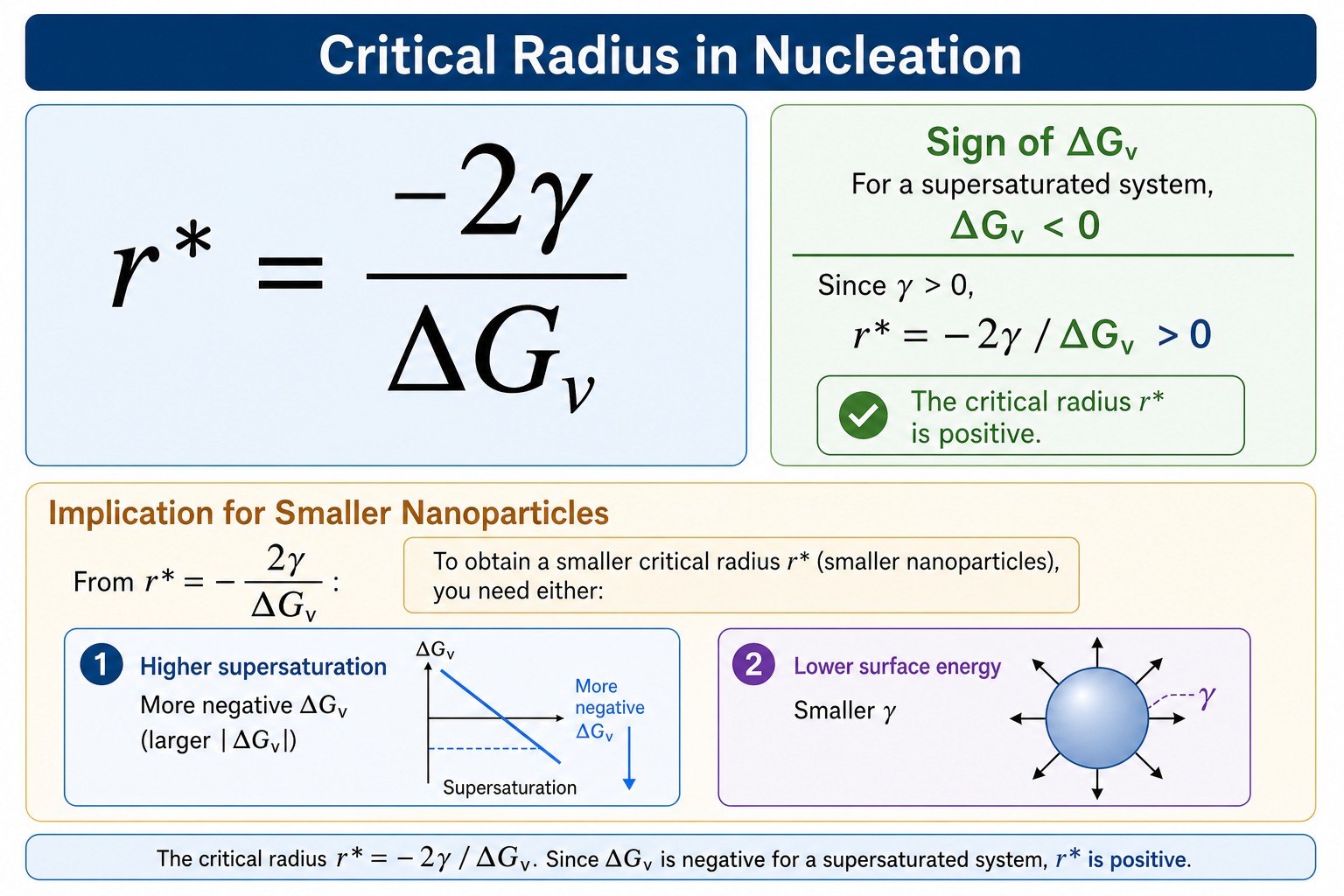
2 Free Energy of Nucleus Formation
The total free energy change ΔG for forming a spherical nucleus of radius r combines a negative volume term (driving nucleation) and a positive surface term (opposing it):
ΔG = (4/3)πr³ΔGv + 4πr²γ
At the critical size r = r*, dΔG/dr = 0. This gives the activation barrier: ΔG* = 16πγ³ / (3ΔGv)²
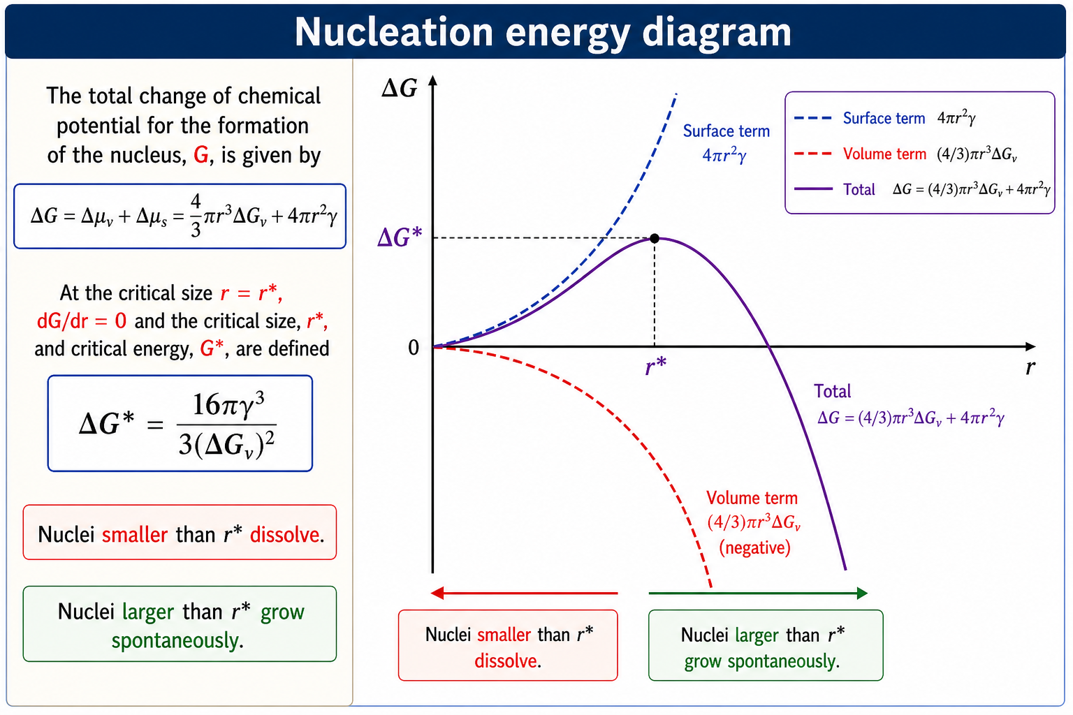
3 Effect of Supersaturation and Temperature
ΔGv increases in magnitude with increasing supersaturation. Supersaturation itself increases as temperature drops below the equilibrium temperature TE. Consequently, lower temperature → higher supersaturation → smaller r* and lower ΔG* — facilitating formation of finer nanoparticles.
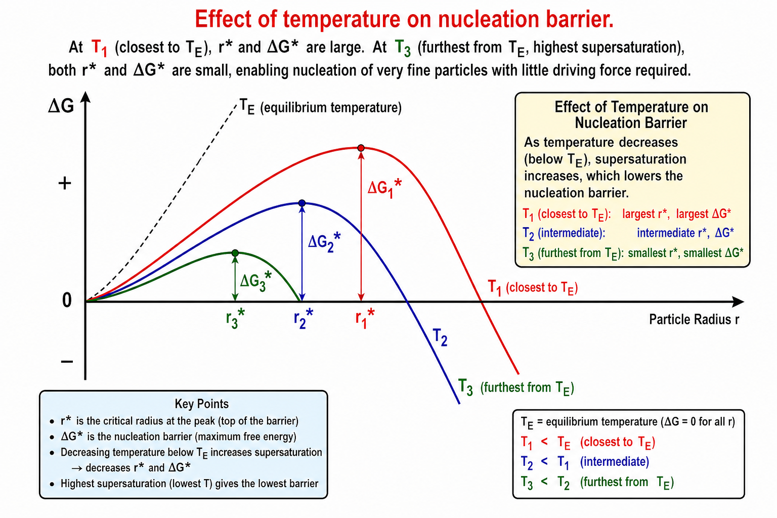
4 Nucleation and Growth Kinetics
When solute concentration rises, no nucleation occurs even above the equilibrium solubility Cs — it only begins when supersaturation reaches the minimum nucleation threshold Cnumin. After the initial nucleation burst, concentration falls below Cnumin and only growth proceeds.
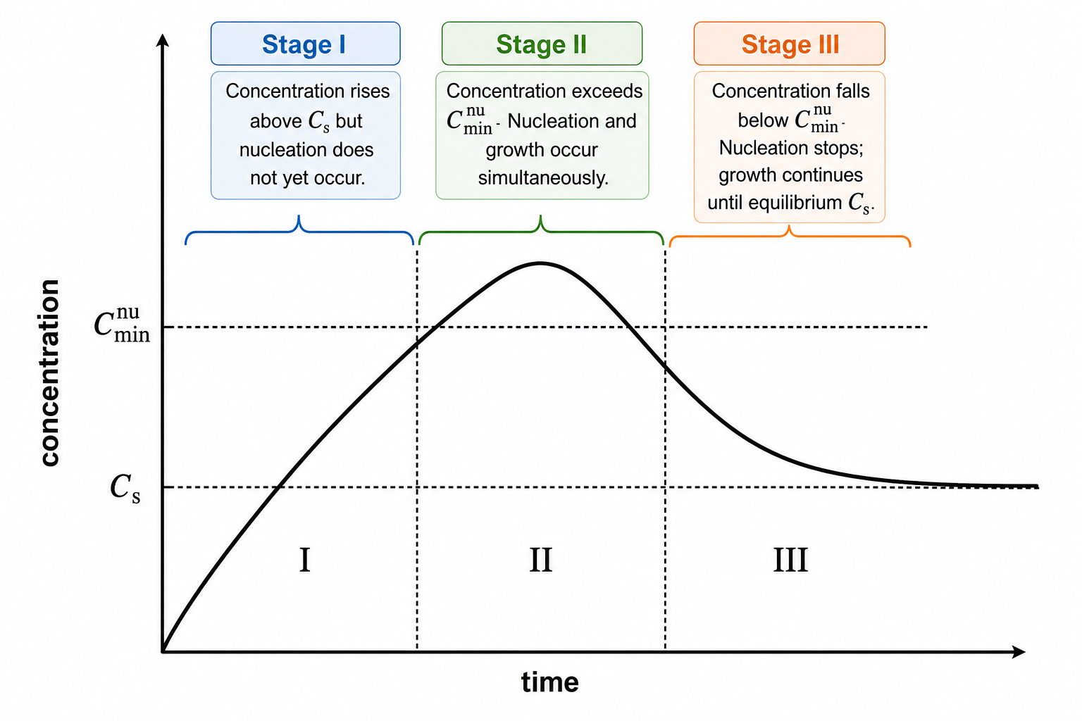
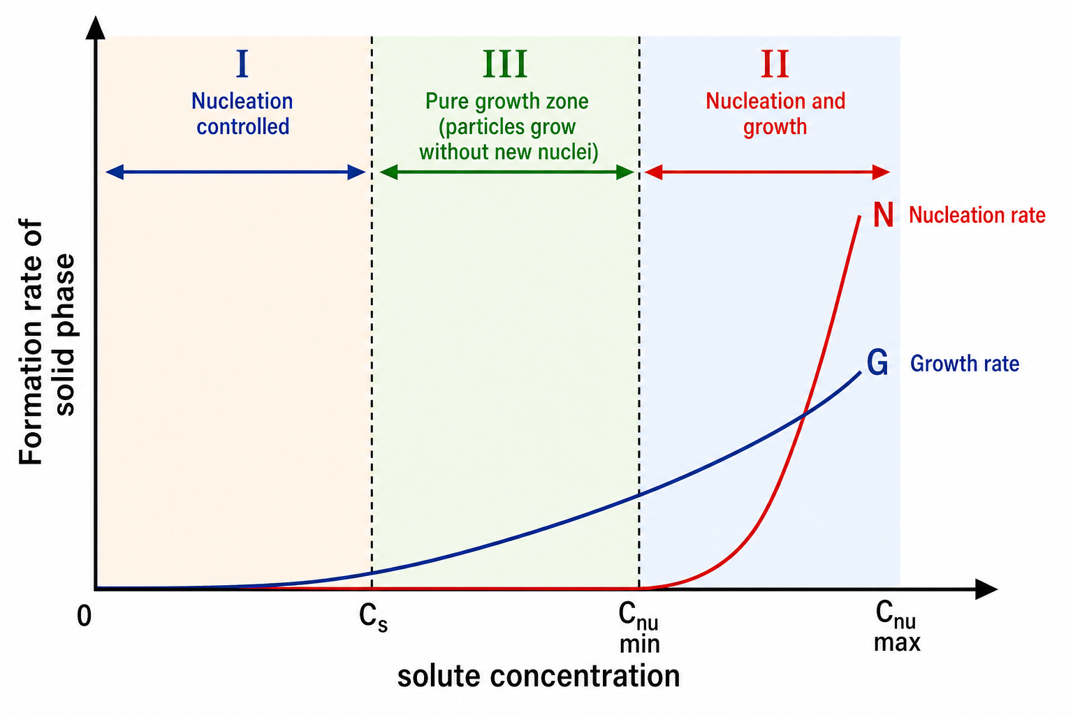
For a narrow size distribution, all nuclei should form simultaneously. In practice: rapidly raise concentration to high supersaturation (burst nucleation) then quickly drop it below Cnumin — all nuclei start at the same time and experience identical subsequent growth conditions, yielding monodisperse particles.
5 1-D Nanostructures: Nanowires and Nanorods
One-dimensional nanostructures are known by many names: whiskers, fibres, fibrils, nanowires, and nanorods (nanotubules and nanocages also belong here). Nanowires generally have a higher aspect ratio than nanorods. Key synthesis routes include:
- Spontaneous growth: evaporation–condensation; vapour-liquid-solid (VLS); stress-induced recrystallisation
- Template-based: electroplating; colloid dispersion; chemical conversion
- Electrospinning
- Lithography
Spontaneous growth is driven by reduction of Gibbs free energy via phase transformation, chemical reaction, or stress release. For nanowires to form, anisotropic growth is essential — certain crystallographic orientations must grow faster than others (different facet growth rates, screw dislocations, or impurity poisoning of specific facets).
6 Crystal Growth & Heterogeneous Nucleation
Growth of nuclei involves four sequential processes: (i) generation of growth species; (ii) diffusion from bulk to the surface; (iii) adsorption onto the surface; (iv) irreversible incorporation into the crystal. When growth occurs on a substrate, this is called heterogeneous nucleation, and two additional steps arise: (v) desorption of by-products; (vi) diffusion of by-products away from the surface.
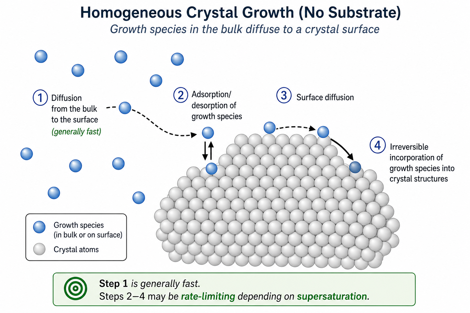
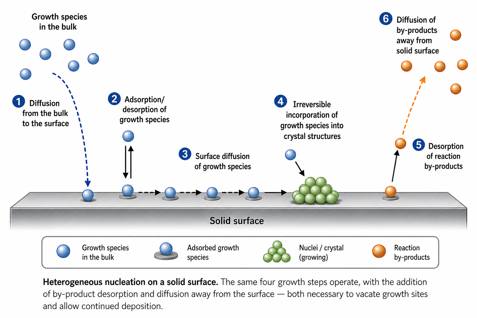
7 Young's Equation and Contact Angle
Whether a deposited phase wets its substrate is governed by the contact angle θ via Young's equation: γsv = γfs + γvf cos θ. Three cases arise:
- θ = 180°: no wetting — new phase sits as a perfect sphere on substrate
- 0° < θ < 180°: partial wetting — energy barrier for heterogeneous nucleation is lower than for homogeneous; γsv < γfs + γvf
- θ = 0°: complete wetting — no energy barrier; equivalent to homoepitaxy
For synthesis of nanoparticles or quantum dots on substrates, θ > 0 is required — the deposit must not wet the substrate completely.
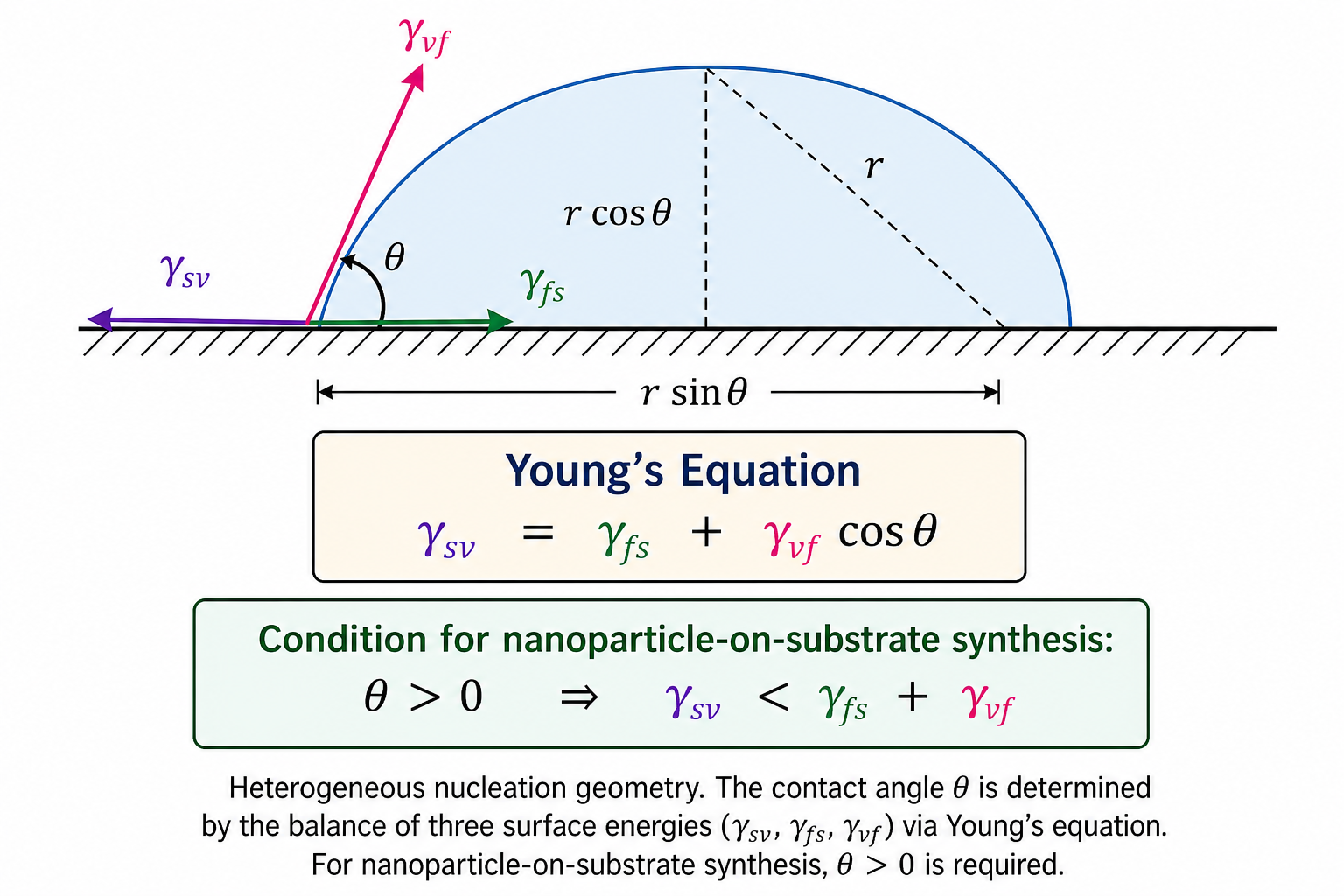
Heterogeneous nucleation dominates in practice because the presence of a substrate or foreign surface dramatically lowers the free energy barrier for nucleus formation. Quantitatively, the heterogeneous nucleation barrier is related to the homogeneous barrier by ΔG*het = ΔG*hom × f(θ), where the geometric factor f(θ) = (2 + cos θ)(1 - cos θ)²/4. This factor depends solely on the contact angle θ between the nucleus and the substrate. For θ = 90° (moderate wetting), f(θ) = 0.5, meaning the energy barrier is halved compared to homogeneous nucleation. As wetting improves and θ decreases toward 0° (complete wetting), f(θ) approaches zero and nucleation becomes essentially barrierless — new phase formation occurs spontaneously on the substrate without any activation energy. Conversely, when θ = 180° (no wetting at all), f(θ) = 1 and the substrate provides no catalytic benefit, reducing to the homogeneous case. This is why, in virtually all real systems, nucleation occurs preferentially on container walls, dust particles, or intentionally introduced substrates rather than spontaneously in the bulk phase.
This principle is exploited deliberately in nanoparticle synthesis through seeded growth methods. When pre-existing seed particles are introduced into a supersaturated solution, they eliminate the nucleation barrier entirely because the new material deposits onto an already-formed solid surface of the same (or compatible) crystal structure. Growth proceeds by epitaxial deposition — atoms from solution add to energetically favourable sites on the seed surface, extending the existing crystal lattice. This is the foundation of core-shell nanoparticle synthesis, where a shell of a different material is grown epitaxially onto a pre-formed core particle (for example, CdSe/ZnS quantum dots, where a ZnS shell is grown on a CdSe core to passivate surface defects and enhance luminescence). Seeded growth also enables shape-controlled synthesis: by choosing seeds with specific crystal facets exposed and using capping agents that selectively bind to certain facets, the growth rate can be made anisotropic, producing nanorods, nanocubes, nanoplates, or branched nanostructures from initially spherical seeds.
A critical challenge in any nucleation-based synthesis is the competition between secondary nucleation and continued growth of existing particles. If supersaturation remains above the critical nucleation threshold after the initial nucleation event, new nuclei continue to form alongside the growing particles. These late-forming nuclei are smaller than the particles that nucleated earlier, and the resulting mixture contains particles of widely varying sizes — a broad, polydisperse size distribution. For controlled synthesis of monodisperse nanoparticles, it is therefore essential to separate the nucleation and growth stages in time. After the initial burst of nucleation, the precursor concentration must drop below the nucleation threshold quickly enough that no secondary nucleation occurs, while remaining above the equilibrium saturation concentration so that the existing nuclei can continue to grow. This separation can be achieved by rapid precursor injection (hot injection), by controlled addition rates, or by using seeded growth where the supersaturation is kept deliberately low — sufficient for growth on existing seeds but insufficient to nucleate new particles.
8 Epitaxial Growth Structures
The lattice match between film and substrate determines the epitaxial structure formed during deposition:
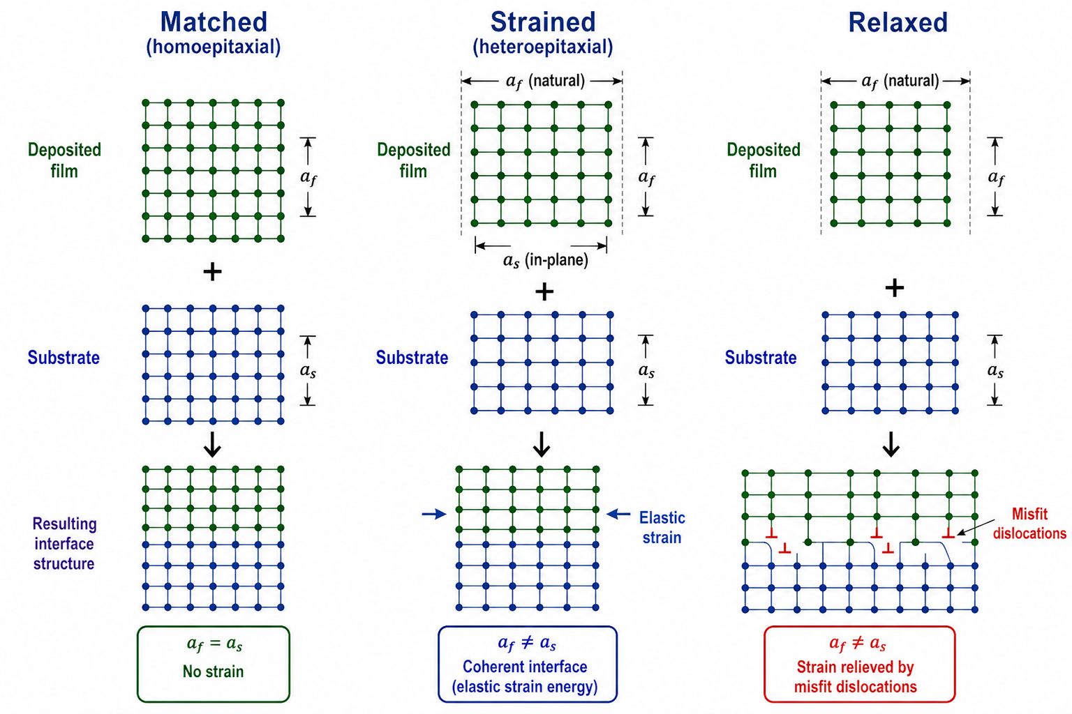
Key Takeaways
- Critical radius r* = −2γ/ΔGv; to make smaller nanoparticles, increase supersaturation or reduce surface energy.
- ΔG = (4/3)πr³ΔGv + 4πr²γ; maximum ΔG* at r* sets the nucleation activation barrier.
- Lower temperature → higher supersaturation → smaller r* and ΔG*.
- Burst nucleation strategy: rapidly reach Cnumax then drop to below Cnumin → simultaneous nucleation → monodisperse particles.
- 1-D nanostructures require anisotropic growth; heterogeneous nucleation on substrates requires θ > 0 (partial wetting).
- Epitaxy: matched → no strain; strained heteroepitaxy → strain energy stored; relaxed → misfit dislocations form.
✦ References & Further Reading
- Cao, G. (2004). Nanostructures & Nanomaterials: Synthesis, Properties & Applications. Imperial College Press.
- Christian, J. W. (2002). The Theory of Transformations in Metals and Alloys. Pergamon.
- Turnbull, D. (1952). Kinetics of solidification of supercooled liquid mercury droplets. Journal of Chemical Physics, 20, 411.
Crystal Growth Mechanisms & Anisotropic Growth
Thin film growth modes, epitaxial relationships, crystal growth as a heterogeneous reaction, the Terrace-Ledge-Kink (TLK / KSV) model, step growth, screw dislocations as continuous growth sources, and anisotropic growth leading to nanowires and nanorods.
Contents
1 Thin Film Growth Modes
From Lecture 11, heterogeneous nucleation depends on the contact angle θ between the new phase and the substrate. The same contact angle governs which of three thin film growth modes operates during deposition. For nanoparticles or quantum dots to nucleate on a substrate, we need θ > 0, so Young's equation gives:
γsv < γfs + γvf
This means the substrate–vapour surface energy is less than the sum of film–substrate and vapour–film surface energies — the deposit does not fully wet the substrate, so it forms islands.
When the deposit does not wet the substrate at all (θ = 180°, i.e. γsv ≪ γfs + γvf), we get pure island or Volmer–Weber growth. When θ = 0 (complete wetting), we get layer-by-layer growth. The three modes are:
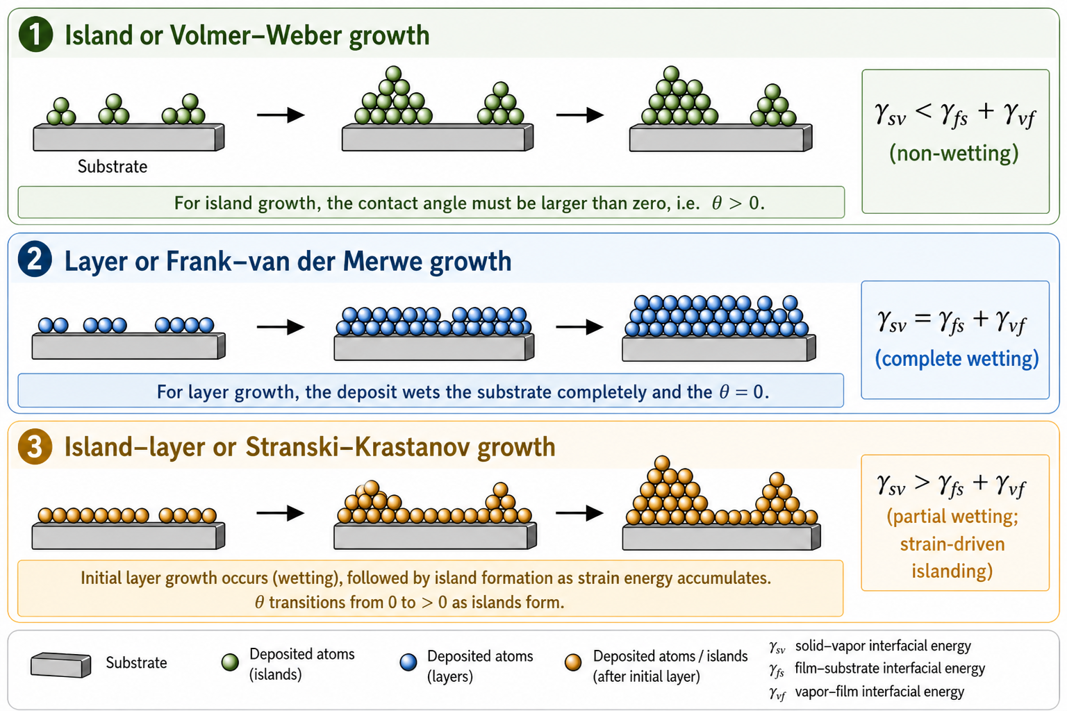
The lattice relationship between the film and substrate matters. Three structural cases arise during deposition:
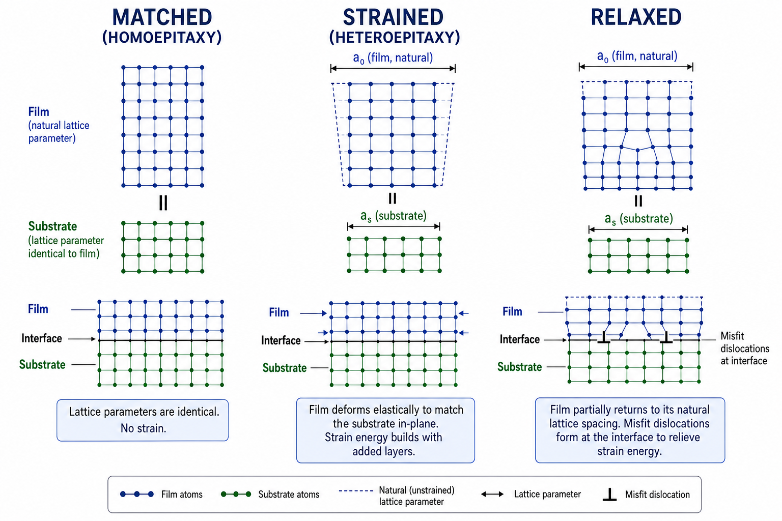
SK growth is the basis of self-assembled quantum dot fabrication. In the InAs/GaAs system, the first few InAs monolayers grow pseudomorphically (strained). As strain energy accumulates proportionally to volume, it eventually exceeds the surface energy advantage of wetting — at which point 3D islands (quantum dots) spontaneously form on top of the wetting layer. This strain-driven transition is the most widely exploited route to uniform, size-controlled quantum dots.
Island-layer growth (SK) involves in-situ developed stress. Initially, deposition follows layer growth mode. When the deposit is elastically strained due to lattice mismatch, strain energy builds up with every new layer. When stress exceeds a critical point, the surface energy of the substrate exceeds the combined surface energy of the deposit and interfacial energy, driving the condition γsv > γfs + γvf and causing island nucleation.
2 Crystal Growth as a Heterogeneous Reaction
Crystal growth can be treated as a heterogeneous reaction occurring at the solid surface. Six sequential steps are involved, and whichever step is slowest controls the overall growth rate:
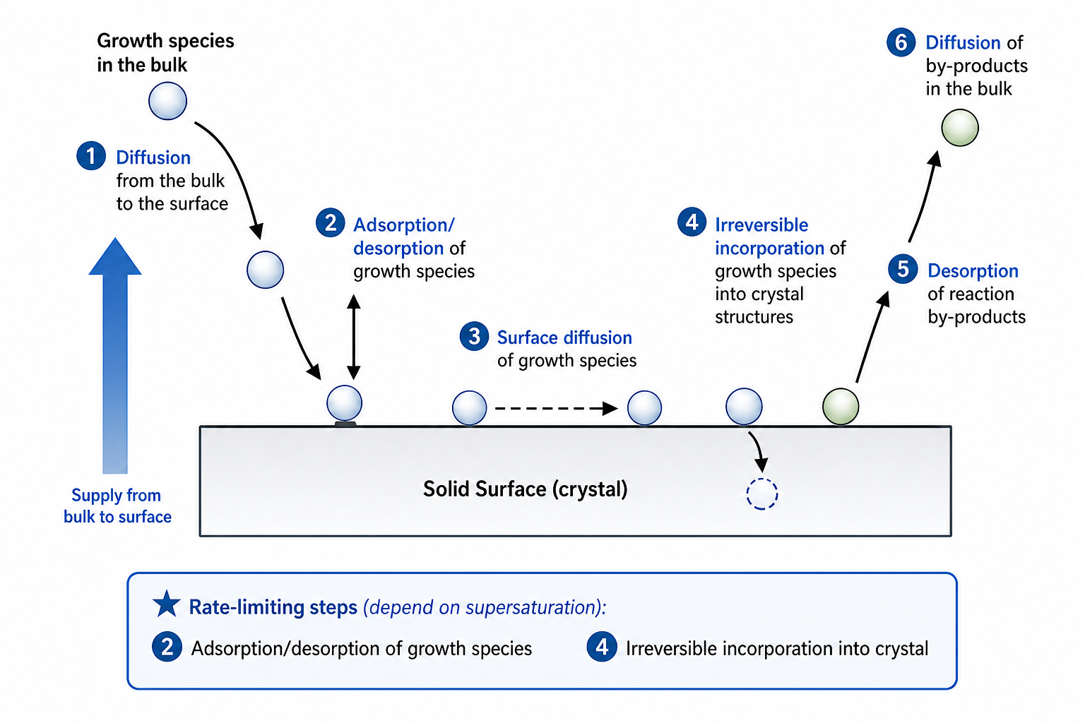
Step 1 — Diffusion from bulk to surface: generally fast, not rate-limiting.
Step 2 — Adsorption/desorption: rate-limiting if supersaturation or concentration of growth species is low.
Step 3 — Surface diffusion: adsorbed species migrate across the surface and may incorporate into a growth site or escape back to the vapour.
Step 4 — Irreversible incorporation: rate-limiting when supersaturation is high and sufficient growth species are present. This step determines the growth rate.
Steps 5 & 6 — By-product desorption and diffusion: by-products must leave the surface to vacate growth sites and allow the process to continue.
3 The Terrace–Ledge–Kink (TLK / KSV) Model
The KSV model (Kossel, Stranski and Volmer, 1920) — also called the Terrace Ledge Kink (TLK) model — describes atomic-scale surface structure and explains crystal growth. The key insight is that a real crystal surface is not smooth, flat or continuous at the atomic scale. These discontinuities — steps, kinks, vacancies — are responsible for crystal growth.
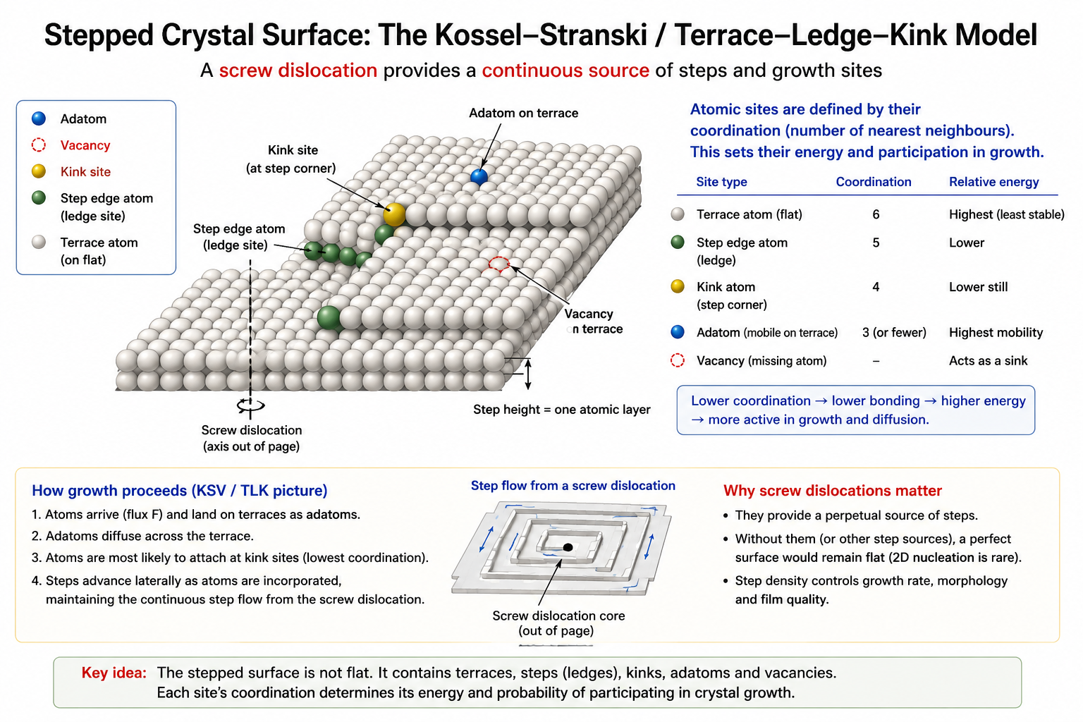
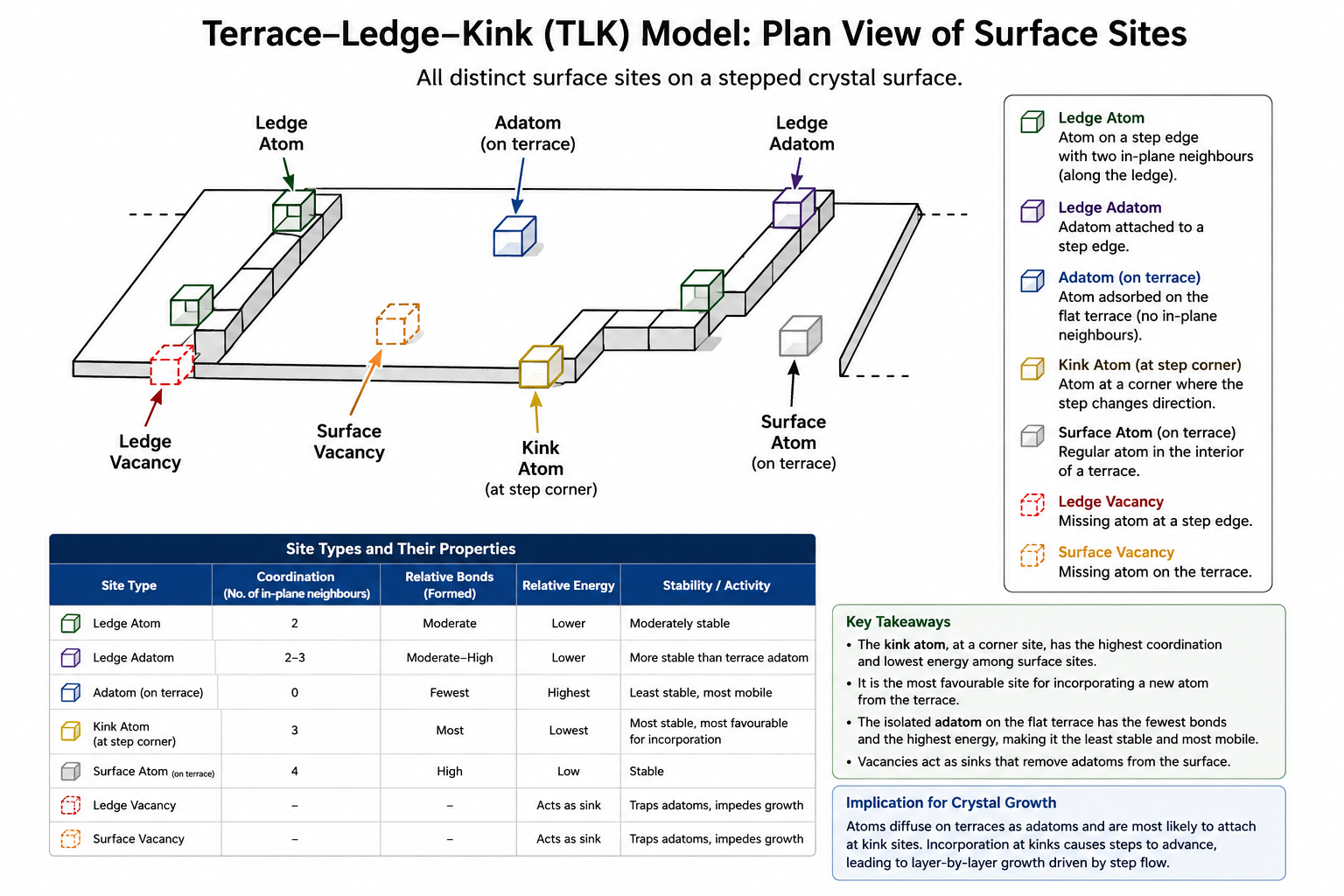
For a simple cubic crystal, each atom in the bulk has coordination number 6 (six chemical bonds). When an atom lands on the surface, it forms fewer bonds depending on which site it occupies. Using a {100} surface as an example:
Adatom on flat terrace: 1 bond — thermodynamically unfavourable, highly mobile. May escape back to vapour.
Atom at a ledge (step) site: 2 bonds — more stable, less mobile.
Atom at a ledge-kink site: 3 bonds — stable, a recognised growth site.
Atom incorporated at a kink site: 4 bonds — most stable site, incorporation is irreversible.
Ledge, ledge-kink, and kink sites are all growth sites. Growth proceeds by the irreversible incorporation of adatoms into these sites, which advances the steps (ledges) laterally across the surface.
STM provides direct experimental confirmation of the TLK model at the atomic scale:
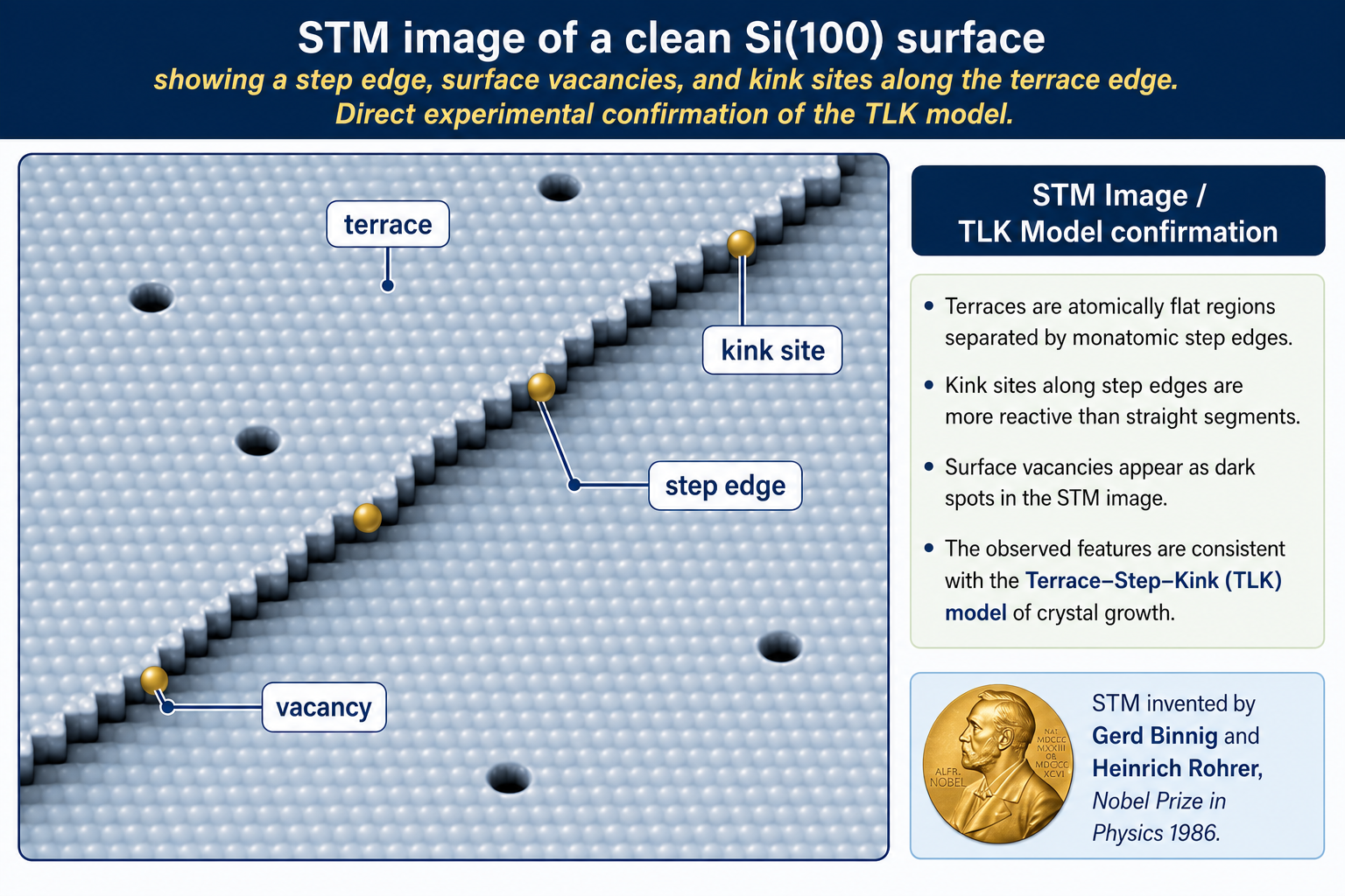
4 Step Growth Mechanism
When an adatom lands on the surface it diffuses randomly. On a flat terrace it forms only 1 bond and is thermodynamically unstable — it may escape back to the vapour. If it diffuses to a ledge site it forms 2 bonds and becomes stable. If it reaches a ledge-kink site (3 bonds) or a kink site (4 bonds), it is irreversibly incorporated into the crystal, and the step advances.
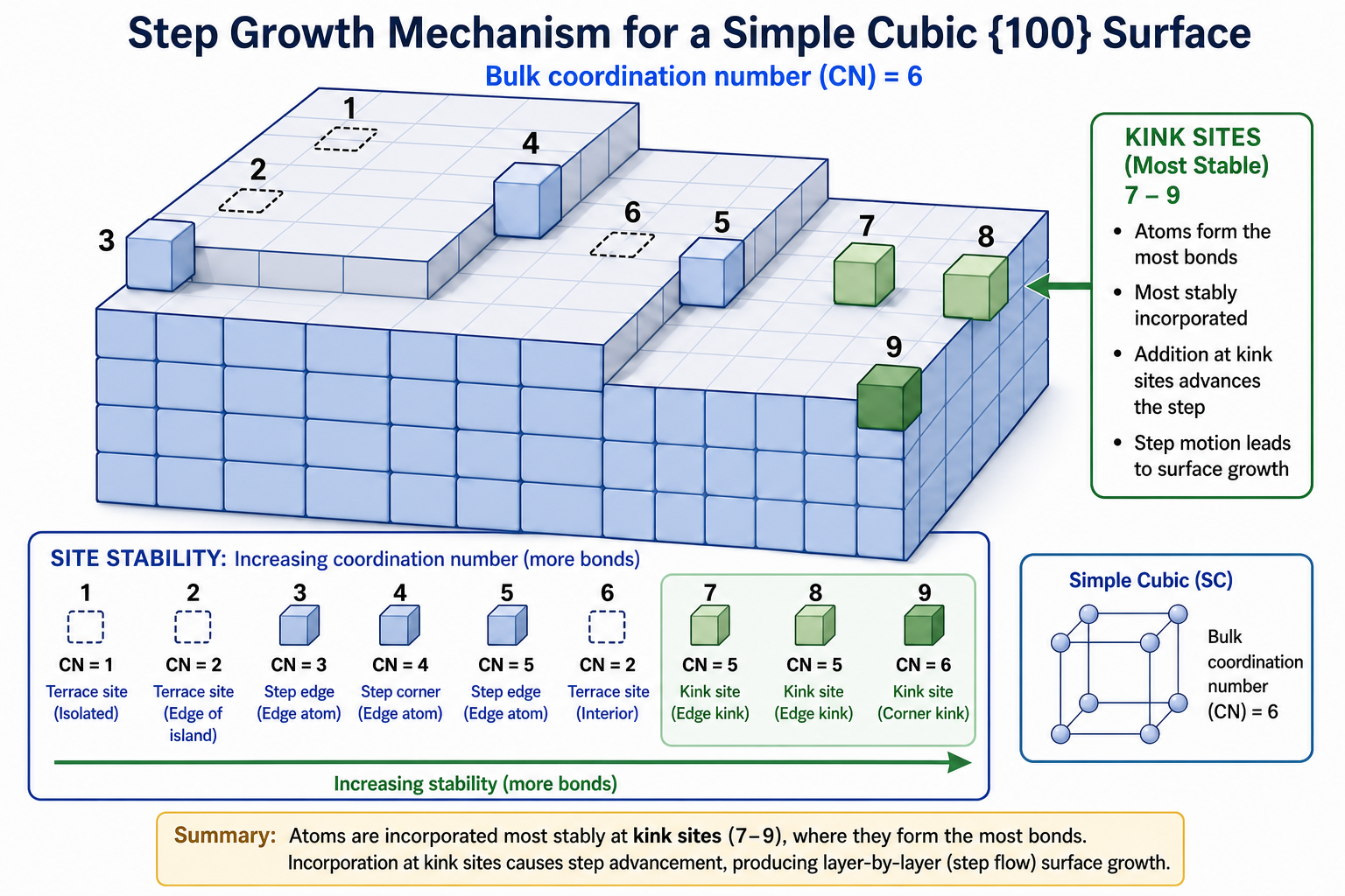
The growth rate on a flat surface depends on step density, which in turn depends on the misorientation of the crystal. A higher step density shortens the average surface diffusion distance an adatom must travel before reaching a growth site — reducing the chance it escapes back to the vapour phase.
If all available ledge and kink sites are filled, stepped growth would halt on a dislocation-free surface. In practice, screw dislocations solve this problem by acting as a continuous self-renewing source of growth steps — allowing stepped growth to continue indefinitely.
5 Screw Dislocation as a Continuous Growth Source
A screw dislocation emerging at the crystal surface creates a permanent step. As atoms incorporate along this step, it spirals around the dislocation core — generating new kink sites continuously without ever being consumed. This mechanism ensures continuous advancement of the growth surface and an enhanced growth rate.
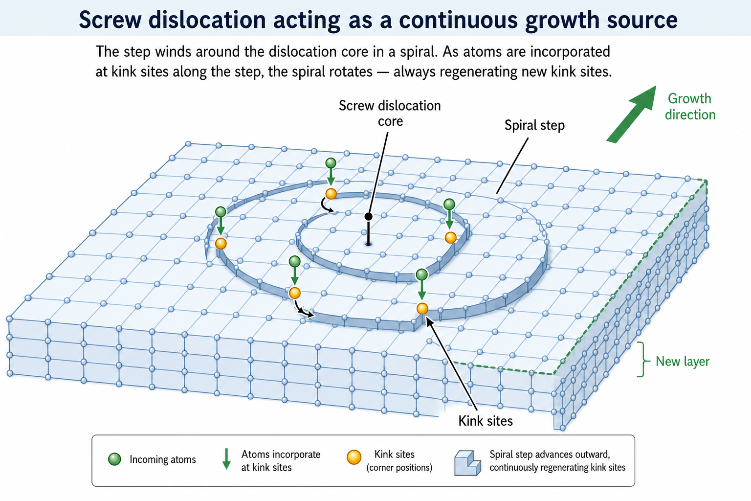
Different crystal facets have significantly different abilities to accommodate dislocations. A facet with more dislocations grows faster. This difference between facets is the fundamental origin of anisotropic crystal growth.
6 Anisotropic Growth → Nanowires and Nanorods
When dislocations concentrate on certain facets, those facets grow preferentially faster — leading to anisotropic morphology. The fundamental rule governing the final shape is:
Facets with fast growth rates grow out of existence — high surface energy faces disappear. Facets with the lowest total surface energy survive in the final equilibrium crystal shape. This is why observed crystal habits expose their lowest-energy faces.
For a simple cubic crystal, we can calculate the surface energy per unit area γ for each low-index face by counting broken bonds. With ε as the bond energy and a as the lattice parameter:
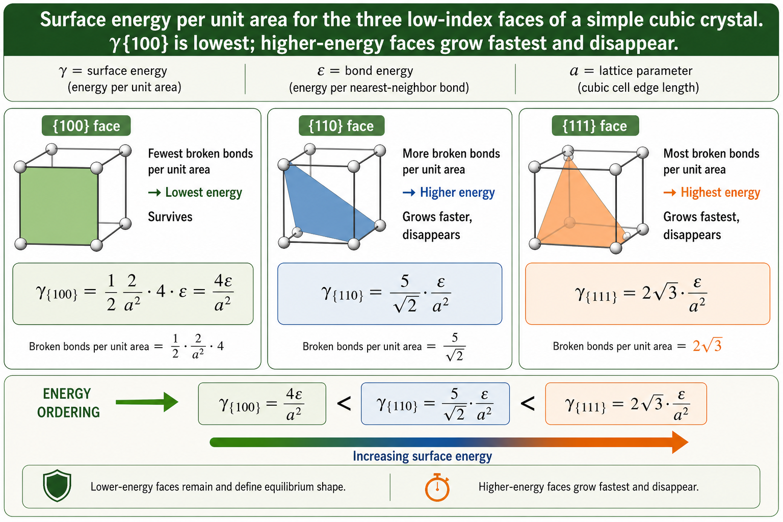
This dislocations-on-specific-facets mechanism is one of three routes to anisotropic growth:
1. Intrinsic difference in facet growth rates — e.g. in silicon (diamond cubic), {111} grows slower than {110}, producing anisotropic crystal habits.
2. Screw dislocations on specific facets — dislocations concentrated on one facet accelerate its growth, creating directional growth → nanowires and nanorods.
3. Surfactant / impurity poisoning of specific facets — selective adsorption of a capping agent or impurity on certain faces blocks growth on those faces, forcing growth in the perpendicular direction. This is the basis of surfactant-directed shape control used extensively in colloidal nanorod synthesis.
Key Takeaways
- Three thin film growth modes: Island/Volmer–Weber (θ > 0, γsv < γfs+γvf), Layer/Frank–van der Merwe (θ = 0), Island-layer/Stranski–Krastanov (starts as layer, converts to islands when accumulated strain drives γsv > γfs+γvf). SK growth is the basis of self-assembled quantum dot synthesis.
- Crystal growth = heterogeneous reaction: six steps from bulk diffusion to by-product removal. Rate-limiting step switches from adsorption (low supersaturation) to incorporation (high supersaturation).
- TLK / KSV model: real crystal surfaces have terraces, ledges, kinks, adatoms, and vacancies. Bond count increases: adatom on terrace (1) → ledge (2) → ledge-kink (3) → kink site (4). Growth proceeds by irreversible incorporation at ledge/kink sites advancing the step.
- Screw dislocation: acts as a continuous self-renewing spiral step source; ensures stepped growth never stops and enhances growth rate.
- Anisotropic growth: fast-growing high-energy faces disappear; slow-growing low-energy faces survive → anisotropic morphology → nanowires/nanorods. Driven by intrinsic rate differences, dislocation density, or surfactant blocking.
✦ References & Further Reading
- Cao, G. (2004). Nanostructures & Nanomaterials: Synthesis, Properties & Applications. Imperial College Press.
- Burton, W. K., Cabrera, N. & Frank, F. C. (1951). The growth of crystals and the equilibrium structure of their surfaces. Phil. Trans. R. Soc. Lond. A, 243, 299–358.
- Binnig, G. & Rohrer, H. (1986). Scanning tunnelling microscopy. IBM Journal of Research and Development, 30(4), 355–369.
Synthesis of 1D Nanomaterials: VLS, SLS & Lithography
Overview of 1D nanomaterial synthesis routes, with deep focus on the Vapor-Liquid-Solid (VLS) and Solution-Liquid-Solid (SLS) growth mechanisms, catalyst design rules, the Au-Si system as a worked example, size control, and nanowire fabrication by lithography.
Contents
1 Routes to 1D Nanomaterial Synthesis
One-dimensional nanomaterials — nanowires, nanorods, nanotubes — can be synthesised by several broad strategies:
(a) Evaporation (or dissolution)-condensation — material is evaporated or dissolved and then condensed into 1D form.
(b) Vapor (or solution)-liquid-solid (VLS / SLS) growth — a liquid catalyst droplet directs and confines growth into one dimension. The focus of this lecture.
(c) Stress-induced recrystallization — internal stress drives directional recrystallisation into whiskers or rods.
(a) Electroplating and electrophoretic deposition into a nanoporous template.
(b) Colloid dispersion, melt, or solution filling of a template.
(c) Conversion with chemical reaction — template reacts chemically to form a new 1D phase.
Electrospinning — a polymer solution is drawn into a nanoscale fibre by an electric field.
Lithography — top-down patterning and etching to define nanowire dimensions. Covered in Section 5.
2 VLS / SLS Growth: The Core Idea
In Vapor-Liquid-Solid (VLS) and Solution-Liquid-Solid (SLS) growth, a second phase material — a catalyst or impurity — is purposely introduced to direct and confine growth to one dimension. Key observable phenomena that define the mechanism:
There are no screw dislocations or other imperfections along the growth direction — so the anisotropic growth mechanism from Lecture 12 is not responsible.
The growth direction is inherently slow. For silicon, the ⟨111⟩ direction grows slowest compared to other low-index directions such as ⟨110⟩ — yet the nanowire grows in ⟨111⟩. This is because the liquid catalyst, not intrinsic anisotropy, is directing growth.
Impurities are always required — no catalyst, no nanowire.
A liquid-like globule is always found at the tip of the nanowire — this is the solidified catalyst droplet, the physical fingerprint of VLS growth.
The catalyst acts as a trap for growth species. Trapped growth species then precipitate at the growth surface — resulting in one-dimensional growth perpendicular to the solid-liquid interface.
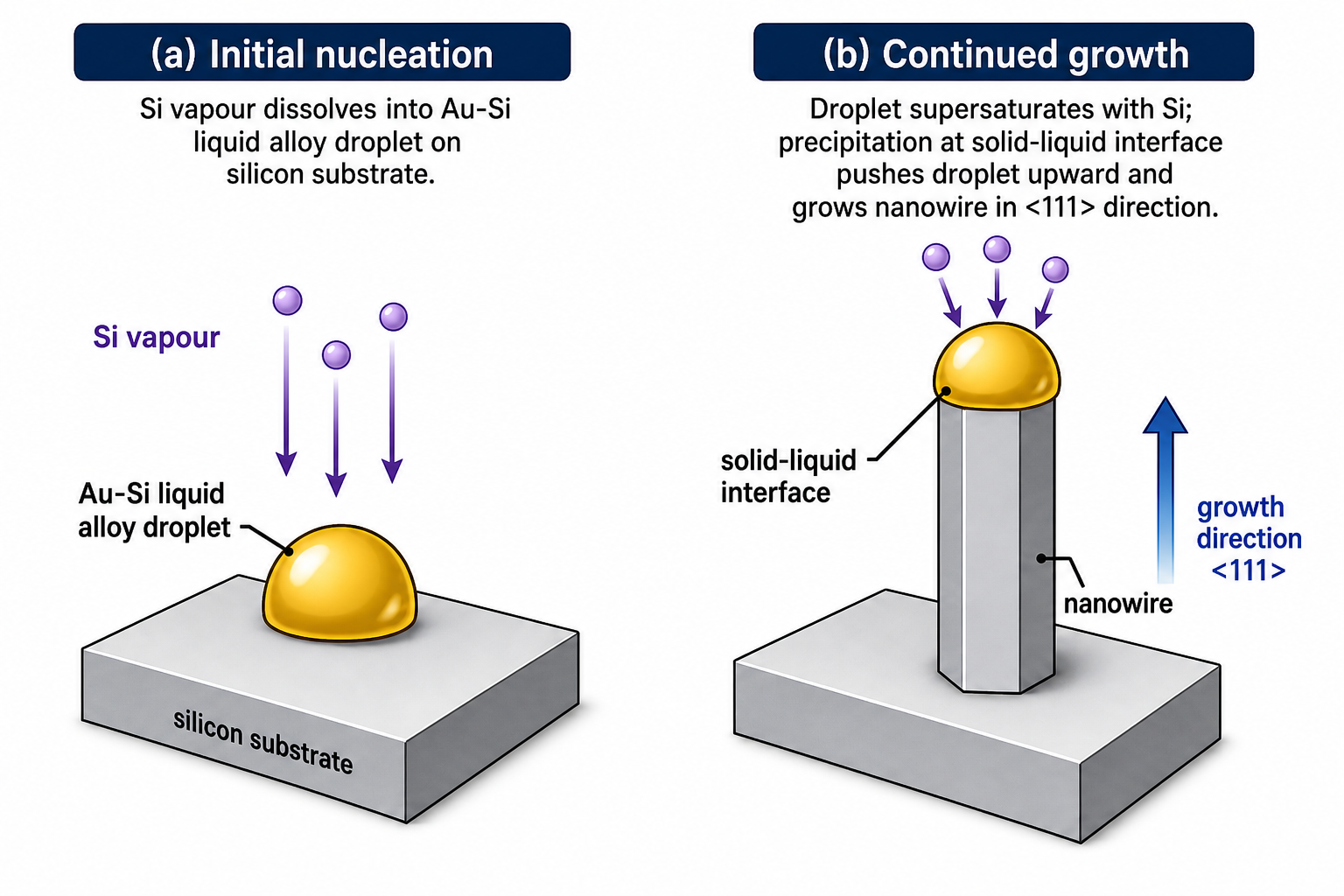
3 Fundamentals of the VLS Method
Six design rules govern catalyst selection and process conditions for successful VLS growth:
1. Liquid solution at deposition temperature. The catalyst or impurity must form a liquid solution with the crystalline material to be grown at the deposition temperature. This is why the Au-Si eutectic is used for Si nanowires — it liquefies at just 363°C, far below Si's melting point of 1414°C.
2. Low distribution coefficient. The distribution coefficient of the catalyst must be small at the deposition temperature — meaning the catalyst strongly prefers the liquid phase and does not incorporate into the growing solid.
3. Low equilibrium vapour pressure over the droplet. The catalyst vapour pressure above the liquid droplet must be very small — otherwise the catalyst evaporates rather than remaining as a droplet to supply growth species.
4. Chemically inert. The catalyst must not react chemically with the nanowire material. It must remain as a distinct liquid phase, not form a compound with the growing crystal.
5. Interfacial energy controls diameter. The interfacial energy between catalyst and substrate plays a critical role. A small wetting angle means a large contact area between droplet and surface — which gives a larger nanowire diameter. Controlling the wetting angle therefore controls the wire width.
6. Compound nanowires: one constituent as catalyst. For compound nanowire growth (e.g. GaAs), one of the constituent elements can itself serve as the catalyst.
7. Controlled unidirectional growth requires crystallographic alignment. For well-defined directional growth, the solid-liquid interface must be crystallographically well-defined — achieved by choosing a single-crystal substrate with the desired crystal orientation.
4 VLS in Practice: Silicon Nanowires with Au Catalyst
The Au-Si system is the canonical example of VLS growth. Understanding the binary phase diagram is essential:
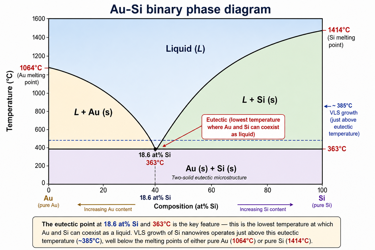
The step-by-step process for growing Si nanowires by VLS:
Step 1 — Catalyst deposition: a thin gold film is sputtered onto a silicon substrate and annealed at ~385°C — above the Au-Si eutectic point of 363°C. Au and Si react to form a liquid Au-Si alloy droplet on the substrate surface.
Step 2 — Growth species supply: Si species are evaporated from a source. The liquid droplet surface has a high accommodation coefficient — it captures impinging Si vapour much more efficiently than the bare crystalline Si substrate. The droplet becomes the preferred deposition site.
Step 3 — Supersaturation: as Si continues to condense onto the droplet surface, the droplet becomes supersaturated with Si. The liquid-vapour interface feeds Si into the droplet faster than it can be incorporated into the crystal.
Step 4 — Precipitation at solid-liquid interface: supersaturated Si diffuses through the liquid droplet from the liquid-vapour interface and precipitates at the solid-liquid interface (between the droplet and the substrate). This precipitation is the crystal growth event.
Step 5 — Unidirectional growth: continued precipitation grows the crystal perpendicularly to the solid-liquid interface — lifting the liquid droplet upward and extending the nanowire. Growth is diffusion-controlled under essentially isothermal conditions. (Isothermal conditions are important because any temperature gradient would drive convection in the droplet and disrupt the controlled diffusion.)
Step 6 — Growth site incorporation: during diffusion through the liquid, the growth species is irreversibly incorporated at a growth site — a ledge, ledge-kink, or kink site — exactly as described in the TLK model from Lecture 12.
A liquid surface is fundamentally different from a crystalline surface. Unlike a crystal where only specific ledge, ledge-kink, and kink sites act as traps, a liquid surface can be considered a "rough" surface — it is composed entirely of ledge, ledge-kink, and kink-equivalent sites. Every point on the liquid surface is a trapping site for impinging growth species. This is why the liquid droplet captures vapour so efficiently and is the preferred deposition site.
If a growth species does not find a preferential site within its residence time on a surface, it escapes back to the vapour. On the liquid droplet surface this essentially never happens — the accommodation coefficient is very high.
5 SLS Growth and Size Control
The Solution-Liquid-Solid (SLS) process is the solution-phase analogue of VLS. The driving motivation is practical: VLS requires high temperatures and vacuum conditions. SLS replaces the vapour source with a solution-phase precursor, enabling growth at significantly lower temperatures — making it more accessible and scalable for many materials.
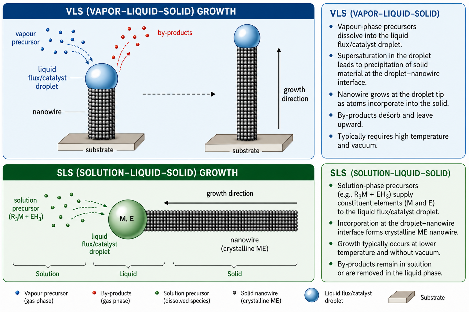
The diameter of nanowires grown by VLS is determined entirely by the size of the liquid catalyst droplets. To control nanowire diameter:
Thinner catalyst film → smaller droplets → smaller diameter nanowires.
The process: coat a thin layer of catalyst on the growth substrate → anneal at elevated temperature → catalyst reacts with substrate to form eutectic liquid droplets. Surface energy minimisation drives the liquid into discrete droplets, and a thinner film produces a higher density of smaller droplets. Since the nanowire diameter equals the droplet diameter, this is the primary handle for diameter engineering.
6 Nanowires by Lithography
Lithography is a top-down approach to nanowire fabrication — the nanowire dimensions are defined by patterning and etching, not by crystal growth. The key advantage is precise dimensional control; the limitation is the minimum feature size achievable by the lithographic process.
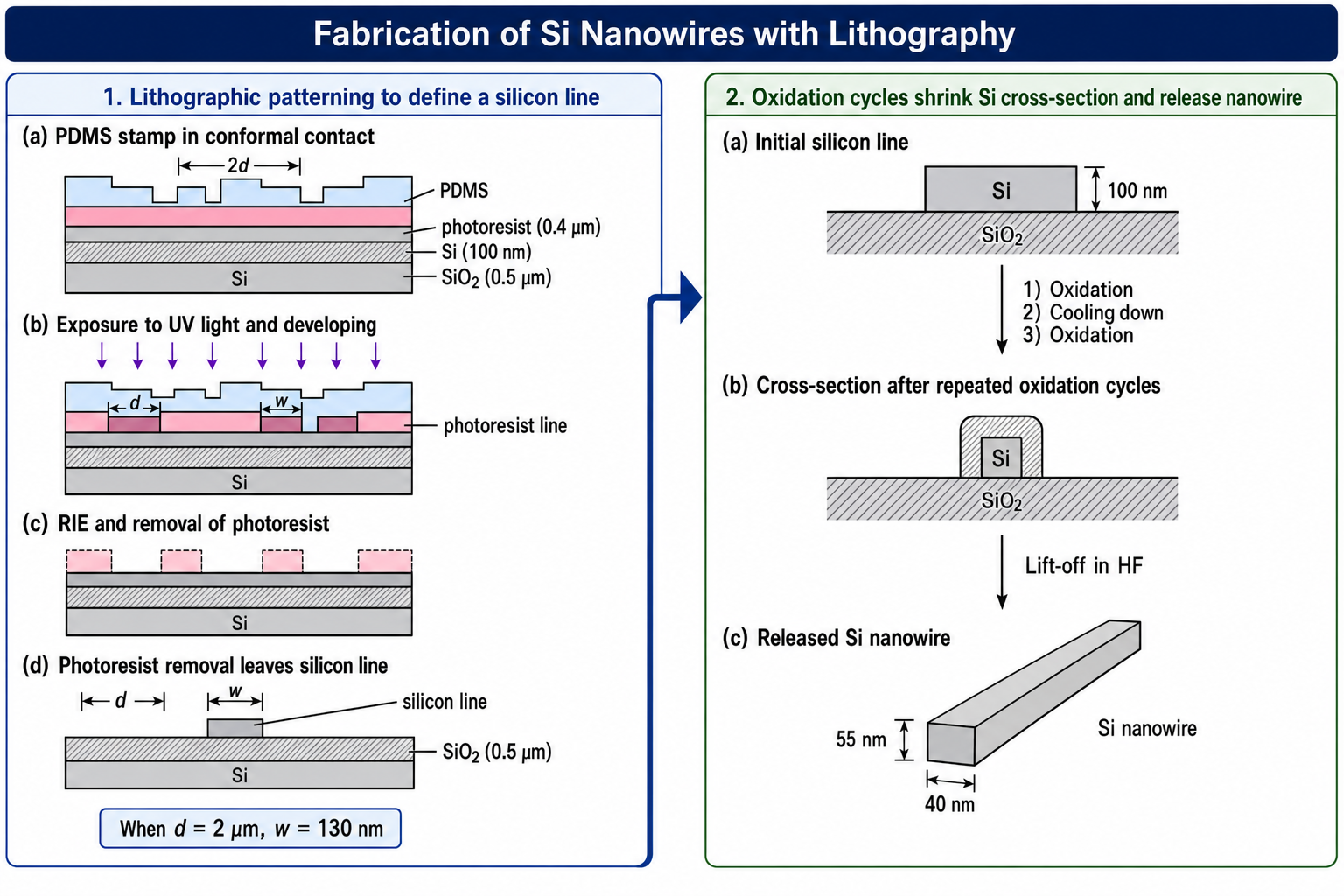
The repeated oxidation–cooling–oxidation sequence converts the outer shell of the Si line into SiO₂, consuming Si and shrinking the cross-section below the lithographically defined size. This is a key trick in silicon nanowire fabrication: lithography defines the pattern; controlled oxidation achieves the nanoscale dimensions. The final HF etch removes the SiO₂ and releases the nanowire.
Key Takeaways
- 1D synthesis routes: spontaneous growth (VLS/SLS, evaporation-condensation, stress-induced recrystallisation), template-based synthesis, electrospinning, and lithography.
- VLS mechanism: catalyst droplet traps growth species from vapour → droplet supersaturates → growth species precipitate at solid-liquid interface → nanowire grows perpendicular to that interface. Liquid tip globule is the fingerprint of VLS.
- Catalyst rules: must form liquid solution at growth temperature, have low distribution coefficient, low vapour pressure, be chemically inert, and have controllable wetting angle.
- Au-Si system: eutectic at 363°C (18.6 at% Si) enables Si nanowire growth at just 385°C — far below pure Si or Au melting points.
- Size control: nanowire diameter = catalyst droplet size; thinner catalyst film → smaller droplets → thinner nanowires.
- SLS vs VLS: SLS uses solution-phase precursors at lower temperatures, avoiding vacuum requirements while retaining the same liquid-mediated growth mechanism.
- Lithographic nanowires: top-down — pattern by photolithography, reduce by thermal oxidation, release by HF etch. Achieves sub-lithographic dimensions.
✦ References & Further Reading
- Cao, G. (2004). Nanostructures & Nanomaterials: Synthesis, Properties & Applications. Imperial College Press. Chapter 4.
- Wagner, R. S. & Ellis, W. C. (1964). Vapor-liquid-solid mechanism of single crystal growth. Applied Physics Letters, 4(5), 89–90.
- Morales, A. M. & Lieber, C. M. (1998). A laser ablation method for the synthesis of crystalline semiconductor nanowires. Science, 279(5348), 208–211.
Thin Film (2D) Growth Methods
An overview of vapor-phase and liquid-based deposition techniques for 2D nanostructures, including nucleation mechanisms, vacuum fundamentals, and physical vapor deposition methods.
Contents
1 Classification of Thin Film Deposition Methods
Thin film (2D) growth methods are broadly divided into two groups: vapor-phase deposition and liquid-based growth. Vapor-phase methods include evaporation, molecular beam epitaxy (MBE), sputtering, chemical vapor deposition (CVD), and atomic layer deposition (ALD). Liquid-based methods include electrochemical deposition, chemical solution deposition (CSD), Langmuir-Blodgett films, and self-assembled monolayers (SAMs).
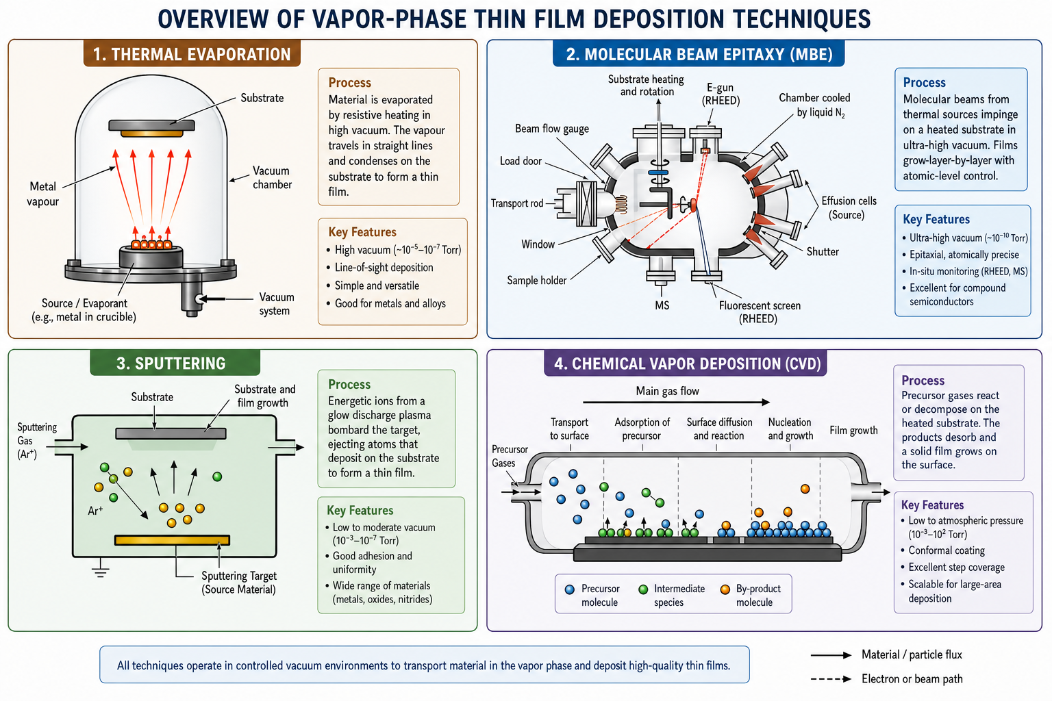
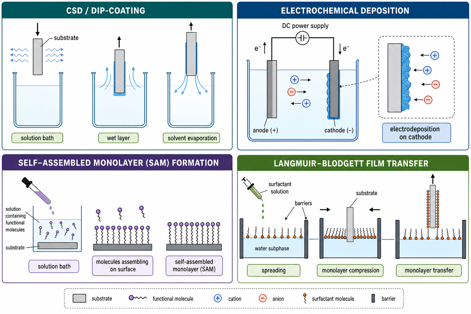
Most film deposition processes are fundamentally heterogeneous in nature, involving heterogeneous chemical reactions, evaporation, adsorption and desorption on growth surfaces, and heterogeneous nucleation and surface growth. Crucially, the vast majority of both film deposition and characterization processes are conducted under vacuum.
2 Nucleation and Film Growth Modes
Growth of thin films always involves nucleation and subsequent growth on the substrate (growth surface). The nucleation process plays a critical role in determining the crystallinity and microstructure of the resultant film. For films in the nanometer thickness range, the initial nucleation step is even more important.
The role of surface energy (γ) governs which of three distinct thin film growth modes is observed:
- Island growth (Volmer–Weber): Growth species preferentially bond to one another rather than to the substrate. Small clusters nucleate directly on the substrate and grow as three-dimensional islands.
- Layer growth (Frank–van der Merwe): Growth species are more strongly attracted to the substrate than to each other. Growth proceeds layer-by-layer, each layer completing before the next begins.
- Island-layer growth (Stranski–Krastanov): After one or a few monolayers form, subsequent growth reverts to island formation. This intermediate mode arises when lattice mismatch accumulates strain in the layers.
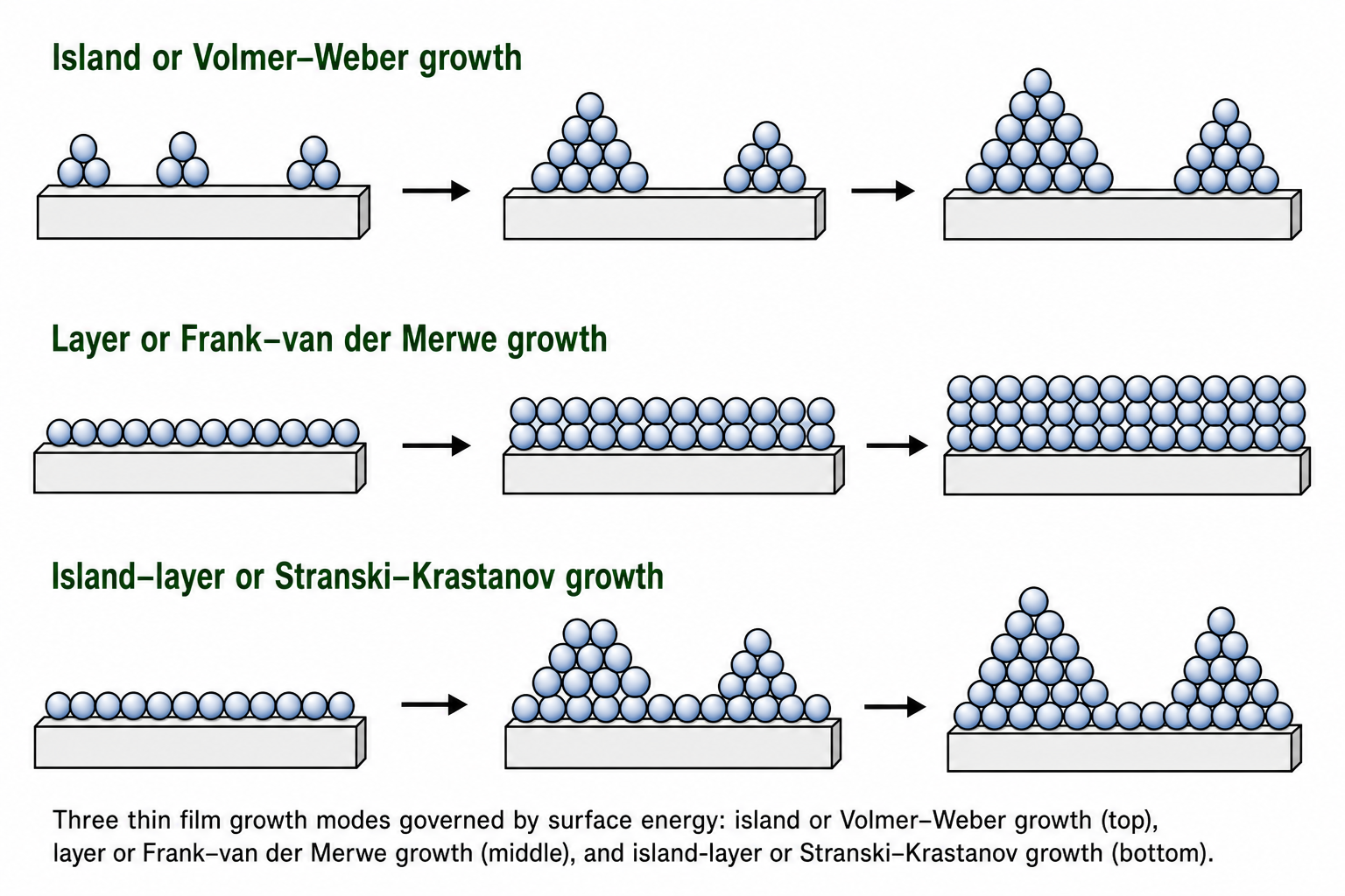
3 Crystal Structure of Deposited Films
Whether a deposited film is single-crystalline, polycrystalline, or amorphous depends on the growth conditions and the substrate.
Single crystal growth requires: (i) a single crystal substrate with a close lattice match; (ii) a clean substrate surface to minimize secondary nucleation; (iii) a high growth temperature to ensure sufficient mobility of growth species; and (iv) a low impinging flux to allow adequate time for surface diffusion, structural relaxation, and proper lattice incorporation before the next species arrive.
Amorphous films result when: (i) a low growth temperature is applied, leaving insufficient surface mobility, or (ii) the influx of growth species is very high so that arriving atoms cannot find energetically favourable growth sites before being buried.
Polycrystalline films form under intermediate conditions — moderate temperature ensures reasonable surface mobility while moderately high impinging flux does not allow full single-crystal registry. Grain size transitions from nanoscale (high disorder) to micron-scale with increasing crystallographic order.
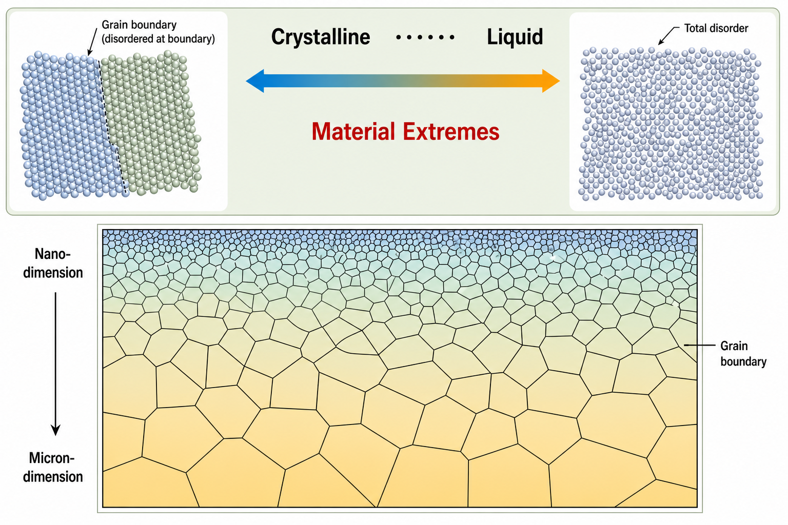
4 Vacuum Technology Fundamentals
The quality of most film deposition and characterization processes depends directly on the quality of vacuum. In a gas phase, molecules are in constant motion, colliding with each other and with container walls. Gas pressure is the result of momentum transfer from gas molecules to the walls and is the primary system variable in vacuum technology.
The mean free path (λmfp) is the mean distance traveled by a molecule between successive collisions and is an important gas property that depends on pressure:
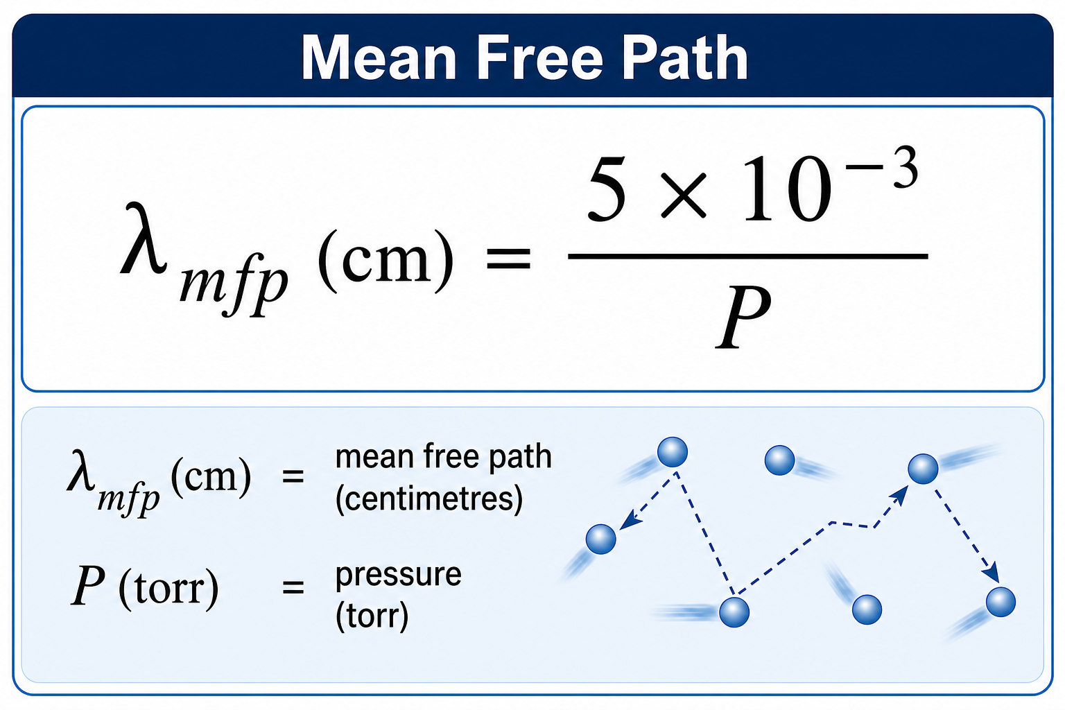
When pressure drops below 10−3 torr, gas molecules in typical film deposition systems virtually collide only with the chamber walls — there is effectively no intermolecular collision. The gas impingement flux (Φ) measures the frequency with which molecules impinge on or collide with a surface:
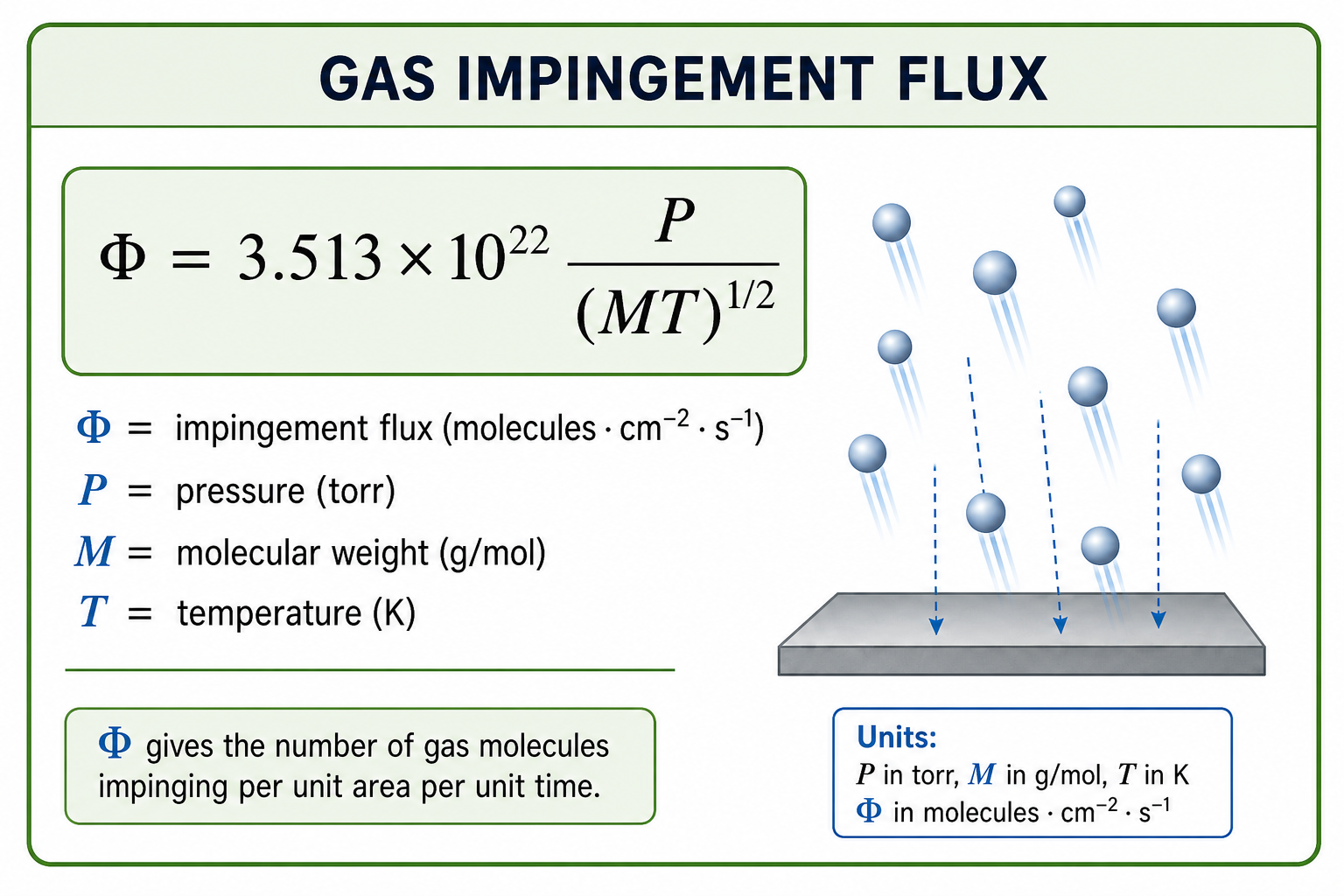
5 Physical Vapor Deposition (PVD)
Physical Vapor Deposition (PVD) transfers growth species from a source or target and deposits them onto a substrate to form a film. The process proceeds atomistically and generally involves no chemical reactions. The main PVD methods are evaporation and sputtering.
In evaporation, material is thermally vaporized (by resistive heating or electron beam impact) and travels in a straight line-of-sight path to the substrate under high vacuum (10−3 to 10−10 torr). The concentration of growth species in the gas phase is controlled by varying source temperature and carrier gas flux. A key limitation is poor conformal coverage over large areas — solutions include using multiple sources or mounting both source and substrates on a shared spherical surface.
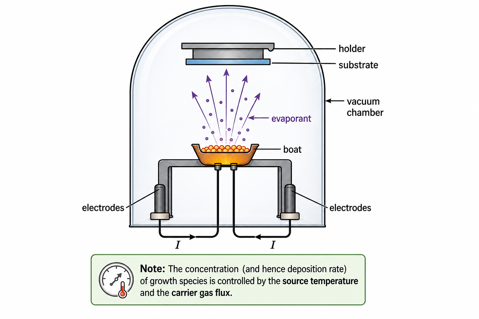
The conceptual framework underlying all thermodynamic nanoparticle synthesis is LaMer's model, which describes three distinct temporal stages. In Stage I (prenucleation), precursors decompose or react in solution, and the concentration of reactive monomers rises steadily. No nucleation occurs because the concentration has not yet reached the critical supersaturation threshold — the system is metastable. In Stage II (burst nucleation), the monomer concentration exceeds the critical supersaturation level, and the nucleation rate increases explosively. A large number of nuclei form in a very short time, rapidly consuming monomers and causing the concentration to drop back below the nucleation threshold. The brevity of this nucleation burst is essential — it ensures that all nuclei form within a narrow time window and therefore begin growth at approximately the same size. In Stage III (growth by diffusion), the monomer concentration remains above the equilibrium saturation level (so growth is thermodynamically favoured) but below the nucleation threshold (so no new nuclei form). Existing particles grow by diffusion of monomers from the bulk solution to the particle surface. The temporal separation of nucleation and growth is the central principle of LaMer's model and the key to achieving monodisperse nanoparticle populations.
After the active growth phase, nanoparticle dispersions can undergo Ostwald ripening (coarsening), a thermodynamically driven process in which larger particles grow at the expense of smaller ones. The driving force is the Gibbs-Thomson effect: smaller particles have higher surface curvature, and therefore higher chemical potential and greater solubility than larger particles. Monomers dissolve preferentially from small particles and redeposit onto large ones, causing the average particle size to increase over time while the total number of particles decreases. The kinetics of this process are described by the LSW theory (Lifshitz-Slyozov-Wagner), which predicts that the average particle radius grows according to the cubic coarsening law: r̄³ ∝ t. The LSW theory also predicts that the particle size distribution, when normalised by the mean radius, approaches a time-independent, self-similar shape with a characteristic maximum at r/r̄ ≈ 1.5 and a sharp cutoff at r/r̄ = 1.5. Ostwald ripening is generally undesirable in nanoparticle synthesis because it broadens the size distribution and increases the average size, but it can be minimised by using strongly binding capping ligands that reduce the rate of monomer exchange between particles and solution.
In contrast to Ostwald ripening, digestive ripening is a process in which the size distribution narrows over time — large particles shrink while small particles grow, driving the system toward a uniform, monodisperse state. This seemingly counterintuitive behaviour (the reverse of Ostwald ripening) occurs when strongly binding ligands are present that preferentially stabilise smaller particles. Because smaller particles have higher surface curvature, the ligand packing density and binding geometry differ from those on larger, flatter surfaces. If the ligand-surface binding energy increases with curvature (as observed with thiols on gold nanoparticles, for example), then smaller particles become thermodynamically more stable than larger ones, inverting the usual size-dependent solubility relationship. Digestive ripening is typically carried out by refluxing a polydisperse nanoparticle dispersion in the presence of excess ligand at elevated temperature, allowing the system to equilibrate toward the thermodynamically preferred narrow size distribution. This technique has been particularly successful in producing highly monodisperse gold, silver, and other noble metal nanoparticles with standard deviations in diameter below 5%.
Key Takeaways
- Thin film growth is divided into vapor-phase (evaporation, MBE, sputtering, CVD, ALD) and liquid-based (electrodeposition, CSD, LB films, SAMs) methods.
- Film deposition is inherently heterogeneous and almost universally conducted under vacuum.
- Three growth modes — Volmer-Weber (island), Frank-van der Merwe (layer), and Stranski-Krastanov (island-layer) — are governed by relative surface energies.
- Crystal structure (single crystal, polycrystalline, amorphous) is controlled by deposition temperature and impinging flux.
- Mean free path λmfp = 5 × 10⁻³/P (cm, torr); below 10−3 torr molecules only collide with walls.
- PVD evaporation operates at 10−3–10−10 torr; concentration is tuned by source temperature and carrier gas flux.
- G. Cao, Nanostructures and Nanomaterials: Synthesis, Properties and Applications, Imperial College Press, 2004.
- M. Ohring, Materials Science of Thin Films, 2nd ed., Academic Press, 2002.
- C.B. Gorham, Introduction to Surface Engineering and Functionally Engineered Materials, Scrivener, 2011.
Sputtering, MBE & CVD
Physical vapour deposition by sputtering, ultra-high-vacuum epitaxy by molecular beam epitaxy, and chemical vapour deposition — the three workhorse techniques for growing nanoscale thin films and coatings.
Contents
1 Sputtering
Sputtering is a physical vapour deposition (PVD) process in which energetic ions — typically Ar+ from a glow-discharge plasma — are accelerated toward a solid target. When an Ar+ ion strikes the target surface with sufficient kinetic energy (typically 100 eV to several keV), it transfers momentum to the near-surface atoms through a cascade of collisions. If the energy transferred to a surface atom exceeds its surface binding energy, the atom is ejected — or "sputtered" — from the target. These ejected atoms travel through the low-pressure chamber (typically 1–100 mtorr of Ar) and condense on the substrate, building up a thin film atom by atom. The sputtering yield — the average number of target atoms ejected per incident ion — depends on the ion energy, the ion-to-target mass ratio, and the surface binding energy of the target material. Typical yields range from 0.5 to 3 atoms per ion for most metals.
In DC sputtering, a constant negative voltage (300–5000 V) is applied to the target, which must be electrically conducting so that the ion current can flow. This limits DC sputtering to metallic targets. For insulating targets — ceramics, oxides, nitrides — charge accumulates on the target surface and extinguishes the plasma. RF sputtering solves this problem by applying an alternating voltage at radio frequency (13.56 MHz); the target is alternately bombarded by ions (negative half-cycle) and neutralised by electrons (positive half-cycle), preventing charge build-up and enabling sputtering of any material, including dielectrics such as SiO2 and Al2O3.
Magnetron sputtering dramatically increases the deposition rate by placing permanent magnets behind the target. The magnetic field confines secondary electrons (emitted when ions strike the target) to helical paths close to the target surface, greatly increasing their path length and hence the probability that each electron will ionise an Ar atom before being lost to the chamber walls. The result is a denser plasma concentrated near the target, higher ion current densities, higher sputtering rates, and the ability to operate at lower Ar pressures (1–5 mtorr instead of 50–100 mtorr). Lower pressure means fewer gas-phase collisions and more energetic arriving atoms, which improves film density and adhesion. Magnetron sputtering is the dominant industrial PVD method for depositing thin films of metals, alloys, and ceramics — applications include metallisation layers in microelectronics, hard coatings (TiN, CrN) on cutting tools, low-emissivity coatings on architectural glass, and magnetic recording media.
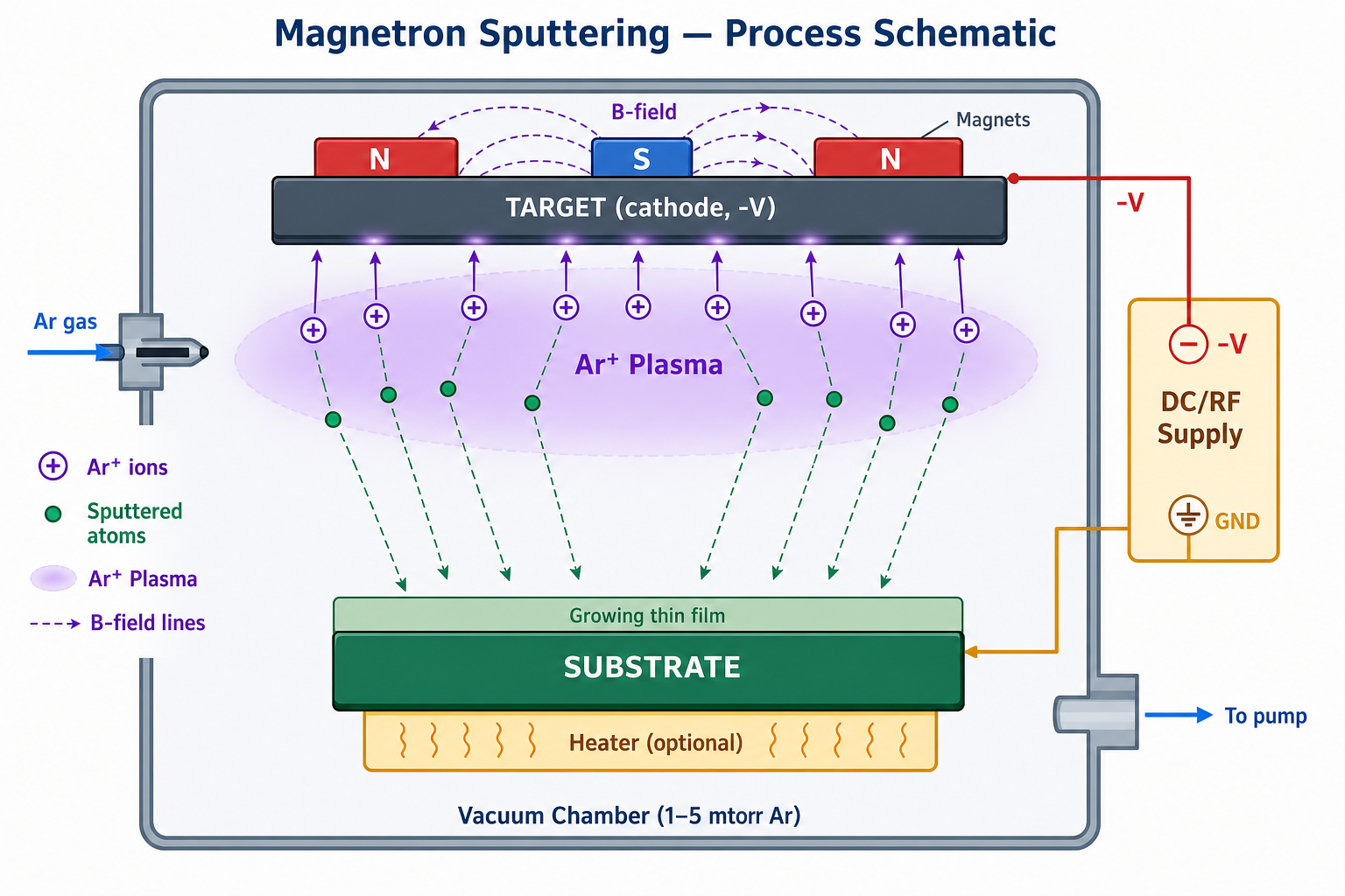
Fig. 15.1 Magnetron sputtering process schematic. Ar⁺ ions from the confined plasma bombard the target (cathode), ejecting target atoms that travel through the low-pressure chamber and condense on the heated substrate. Permanent magnets behind the target create a magnetic field that traps secondary electrons near the target surface, intensifying the plasma and increasing the sputtering rate.
2 Molecular Beam Epitaxy (MBE)
Molecular Beam Epitaxy is the ultimate precision technique for thin film growth. It operates under ultra-high vacuum (UHV), typically below 10−10 torr, ensuring that the mean free path of atoms vastly exceeds the source-to-substrate distance — so the evaporated atoms travel in straight-line molecular beams with no gas-phase collisions. The source materials — ultra-pure elements — are heated in individual Knudsen effusion cells (small crucibles with a precisely controlled orifice) until they sublimate or evaporate. Mechanical shutters in front of each cell allow the beam flux to be switched on or off within a fraction of a second, enabling atomic-layer-level control of composition. The substrate is heated (typically 400–700 °C for III-V semiconductors) to provide sufficient surface diffusion for arriving atoms to find energetically favourable lattice sites, promoting single-crystal epitaxial growth.
Growth is monitored in real time by Reflection High-Energy Electron Diffraction (RHEED). A glancing-incidence electron beam strikes the growing surface; the diffraction pattern on a fluorescent screen provides instantaneous information about surface crystallography, roughness, and growth mode. Periodic oscillations in the RHEED intensity correspond to the completion of successive monolayers — each oscillation period equals the time to deposit one atomic layer. This monolayer-resolution feedback makes MBE uniquely suited for growing semiconductor heterostructures with atomically abrupt interfaces: quantum wells (e.g. GaAs/AlGaAs), superlattices, and quantum dot arrays. The principal disadvantages of MBE are its extremely slow growth rate (typically 0.1–1 μm/hr), the need for UHV infrastructure, and the high capital cost — making it primarily a research and specialty-device tool rather than a high-volume manufacturing method.
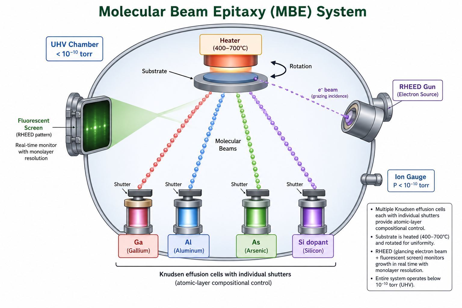
Fig. 15.2 Molecular Beam Epitaxy (MBE) system. Multiple Knudsen effusion cells (Ga, Al, As, Si dopant) each with individual shutters provide atomic-layer compositional control. The substrate is heated and rotated for uniformity. RHEED (glancing electron beam + fluorescent screen) monitors growth in real time with monolayer resolution. The entire system operates below 10⁻¹⁰ torr.
3 Chemical Vapour Deposition (CVD)
Chemical Vapour Deposition differs fundamentally from PVD methods in that the film-forming species arrive at the substrate as gaseous precursor molecules, which then react or thermally decompose on the heated substrate surface to deposit a solid film. The by-products are volatile and are carried away in the gas exhaust. Because the precursors are delivered from the gas phase and the reaction occurs on every exposed surface, CVD can coat complex three-dimensional geometries conformally — including deep trenches, high-aspect-ratio vias, and the insides of tubes — which is impossible with the line-of-sight deposition characteristic of sputtering and evaporation.
Several important variants of CVD exist, each optimised for different applications. Thermal CVD (also called conventional or atmospheric-pressure CVD) uses substrate heating alone (typically 600–1200 °C) to drive the decomposition reaction; it is used for silicon epitaxy from SiH4 or SiCl4 and for depositing polycrystalline silicon, SiO2, and Si3N4. Low-Pressure CVD (LPCVD) operates at 0.1–10 torr, which improves film uniformity across large-area substrates by ensuring the process is surface-reaction-limited rather than transport-limited. Plasma-Enhanced CVD (PECVD) uses a radio-frequency plasma to dissociate precursor molecules at much lower substrate temperatures (200–400 °C), enabling deposition on temperature-sensitive substrates such as polymers, aluminium interconnects, and completed CMOS wafers. Metal-Organic CVD (MOCVD) uses metal-organic precursors such as trimethylgallium (TMGa) and arsine (AsH3) to grow compound semiconductors (GaN, InP, AlGaAs) for LEDs, laser diodes, and solar cells at industrial throughput.
The key process parameters in CVD are substrate temperature, total pressure, precursor partial pressures, and gas flow rates. Temperature governs the decomposition kinetics and surface diffusion; pressure determines the boundary-layer thickness and mass-transport rate; flow configuration affects uniformity. CVD is the method of choice for depositing diamond films (from CH4/H2 mixtures), growing carbon nanotubes (from C2H2 or CH4 over Fe/Co/Ni catalyst particles), synthesising large-area graphene on Cu foil (from CH4 at ~1000 °C), and producing silicon carbide and gallium nitride epitaxial layers for power electronics. The ability to scale to large-area, high-throughput deposition while maintaining conformal coverage makes CVD the most widely used thin film deposition technique in semiconductor manufacturing.
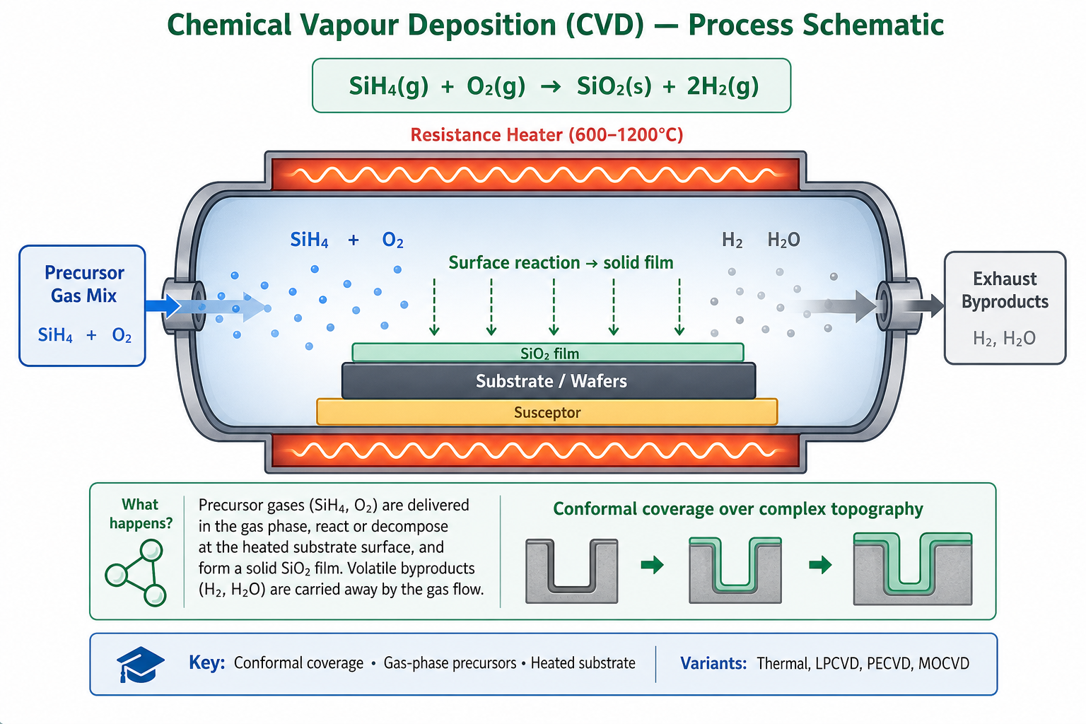
Fig. 15.3 Chemical Vapour Deposition (CVD) process. Precursor gases (e.g. SiH₄ + O₂) flow into a heated reactor tube, where they react or decompose on the substrate surface to form a solid film (e.g. SiO₂). Volatile byproducts (H₂, H₂O) are carried away in the exhaust. The gas-phase delivery gives conformal coverage over complex 3D topography.
4 PVD vs CVD — A Comparison
Physical vapour deposition methods (sputtering, MBE, evaporation) and chemical vapour deposition represent two fundamentally different approaches to thin film growth, and the choice between them is governed by the application requirements. PVD is inherently a line-of-sight process: atoms travel in straight lines from source to substrate, so shadowed regions receive no coating and step coverage over topography is poor. CVD, by contrast, delivers precursors from the gas phase and deposits wherever the reaction conditions are met, giving conformal coverage even in high-aspect-ratio features. Vacuum requirements differ dramatically: MBE demands UHV (10−10 torr), sputtering operates at 1–100 mtorr, while CVD can operate from atmospheric pressure down to ~0.1 torr. Growth rates span three orders of magnitude — MBE at ~0.1 μm/hr, sputtering at 0.1–1 μm/min, and CVD at 0.01–10 μm/min depending on variant. Film quality also differs: MBE produces the highest crystalline perfection (single-crystal epitaxial films with atomically abrupt interfaces), sputtering produces dense polycrystalline or amorphous films with excellent adhesion, and CVD films range from amorphous to single-crystal depending on temperature and precursor chemistry. In practice, all three techniques are complementary — modern device fabrication routinely uses sputtering for metallisation, CVD for dielectrics and barrier layers, and MBE or MOCVD for active semiconductor heterostructures.
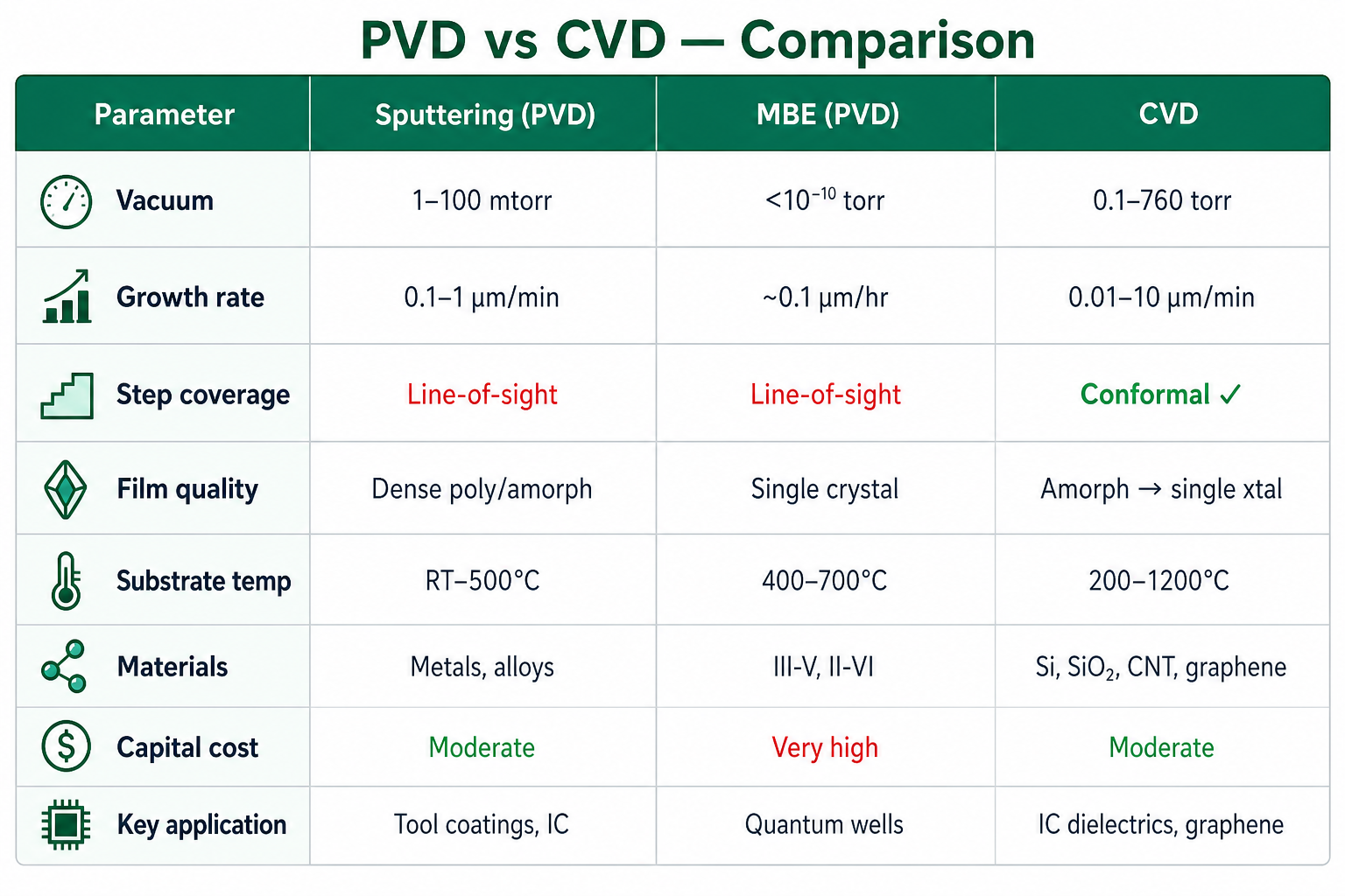
Fig. 15.4 Side-by-side comparison of the three major thin film deposition techniques. Sputtering and MBE (PVD) offer line-of-sight deposition with different vacuum and quality trade-offs; CVD provides conformal coverage and the widest range of operating conditions.
Key Takeaways
- Sputtering ejects target atoms by Ar+ ion bombardment; DC sputtering works for conductors, RF sputtering for insulators, and magnetron sputtering (magnetic electron confinement) boosts rate and lowers operating pressure.
- MBE operates in ultra-high vacuum (10−10 torr) with Knudsen cell sources and RHEED monitoring, achieving monolayer-precision epitaxial growth — ideal for quantum wells and superlattices but slow and expensive.
- CVD uses gaseous precursors that react on a heated substrate; variants (thermal, LPCVD, PECVD, MOCVD) trade temperature, pressure, and plasma activation to suit different materials and substrates.
- CVD provides conformal coverage of 3D topography; PVD (sputtering, MBE) is line-of-sight.
- Growth rates span MBE (~0.1 μm/hr) to sputtering (~0.1–1 μm/min) to CVD (~0.01–10 μm/min); crystalline quality follows the reverse order.
- Key CVD applications: silicon epitaxy, diamond films, carbon nanotubes, graphene, compound semiconductors (GaN, GaAs) for LEDs and lasers.
- M. Ohring, Materials Science of Thin Films, 2nd ed., Academic Press, 2002.
- G. Cao, Nanostructures and Nanomaterials: Synthesis, Properties and Applications, Imperial College Press, 2004.
- D.L. Smith, Thin-Film Deposition: Principles and Practice, McGraw-Hill, 1995.
Liquid-Based Growth, Bulk Nanomaterials & Severe Plastic Deformation
Sol-gel dip and spin coating, electrodeposition of nanocrystalline metals, powder consolidation via pressure sintering and SPS, and severe plastic deformation techniques including ECAP.
Contents
1 Evaporation vs. Sputtering — A Comparison
Evaporation operates at very low pressures (~10−6 torr) with no intermolecular gas collisions, while sputtering operates at ~100 mtorr and involves significant gas-phase collisions. Evaporation is a near-equilibrium thermodynamic process; sputtering is not. Sputtered films show better substrate adhesion and can handle multicomponent targets more faithfully than evaporation. Evaporation tends to produce larger grains; sputtering produces smaller, more uniform grains.
2 Liquid-Based Growth: Sol-Gel Dip Coating
The most commonly used liquid-based methods for thin film deposition are spin coating and dip coating. In dip coating, a substrate is immersed in a solution and withdrawn at a constant speed. As the substrate is pulled upward, solution is entrained, and a balance between viscous drag and gravitational forces determines the final film thickness.
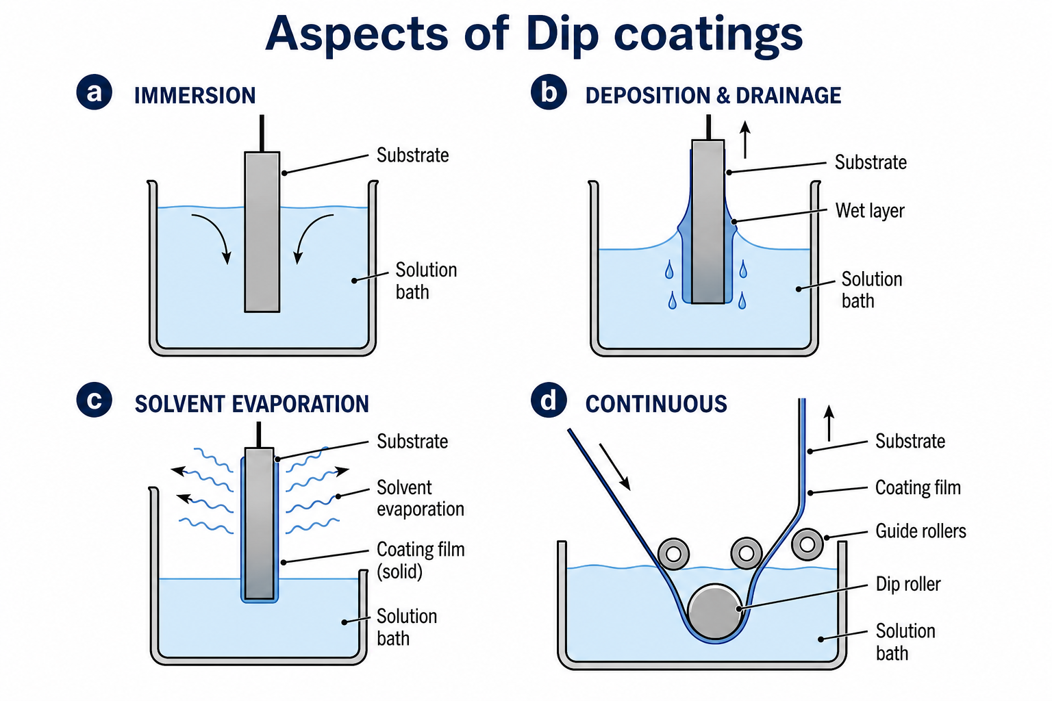
Drying of sol-gel coatings proceeds simultaneously with continuous condensation and solidification of the network. These competing processes generate capillary pressure and constrained shrinkage stresses that can collapse the gel structure or form cracks in the resultant film — a key challenge in producing thick, crack-free coatings.
The sol-gel process is built on two competing reactions: hydrolysis and condensation. In hydrolysis, a metal alkoxide precursor M(OR)n reacts with water to replace an alkoxy group with a hydroxyl: M(OR)n + H2O → M(OH)(OR)n−1 + ROH. In condensation, two hydroxyl-bearing species link together to form a metal-oxygen-metal bridge: M–OH + HO–M → M–O–M + H2O (water condensation) or M–OH + RO–M → M–O–M + ROH (alcohol condensation). The relative rates of hydrolysis and condensation determine the gel morphology: when hydrolysis is fast relative to condensation (e.g. under acidic catalysis), linear or weakly branched polymeric chains form, producing a polymeric gel with small pores and high surface area. When condensation is fast relative to hydrolysis (e.g. under basic catalysis), highly branched clusters nucleate and grow as discrete colloidal particles, producing a particulate gel. Controlling the water-to-alkoxide ratio, pH, solvent, and temperature therefore gives direct control over the final film or powder morphology.
The mechanics of film formation differ between dip coating and spin coating. In dip coating, the entrained film thickness h is governed by the balance between viscous drag (pulling liquid upward with the substrate) and gravity plus surface tension (draining liquid downward). The Landau-Levich equation captures this balance: h ∝ (ηv)2/3 / (γ1/6(ρg)1/2), where η is viscosity, v is withdrawal speed, γ is surface tension, ρ is density, and g is gravitational acceleration. Thicker films are obtained by increasing viscosity or withdrawal speed. In spin coating, the final film thickness scales as h ∝ 1/√ω, where ω is the angular velocity of the spinning substrate. Higher spin speeds produce thinner, more uniform films. This simple inverse-square-root dependence makes spin coating highly reproducible and is the reason it dominates laboratory-scale sol-gel film preparation, while dip coating is preferred for large-area and non-planar substrates.
3 Spin Coating
Spin coating involves four stages: delivery of solution onto the substrate centre, spin-up, spin-off, and evaporation. After delivery, centrifugal forces drive the liquid radially outward (spin-up). Excess liquid is expelled at the substrate edge (spin-off). The remaining thin film dries as solvent evaporates, leaving a uniform coating whose thickness is controlled by viscosity and spin speed.
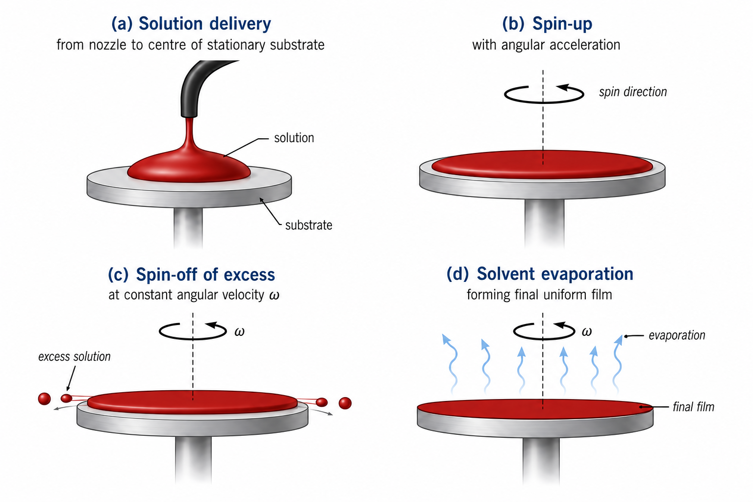
4 Making Bulk Nanomaterials
Two fundamental approaches exist for making bulk nanostructured materials. Bottom-up synthesis inherently produces clean, precise nanostructures but is not easily scalable and reproducibility in terms of porosity, inhomogeneous microstructures, and grain size distribution remains a challenge. Top-down methods (mechanical deformation, milling) are relatively inexpensive and scalable but do not generate a high-quality, defect-free nanostructure and require intensive characterisation.
5 Electrodeposition of Nanocrystalline Metals
Electrochemical deposition is a powerful bottom-up route for producing fully dense nanocrystalline metallic films and coatings. A classic example is nanocrystalline nickel produced by pulsed electrodeposition (Integran Technologies). The Ni anode dissolves as Ni²⁺ ions into the electroplating solution; these ions migrate to the wafer cathode and deposit as metallic Ni.
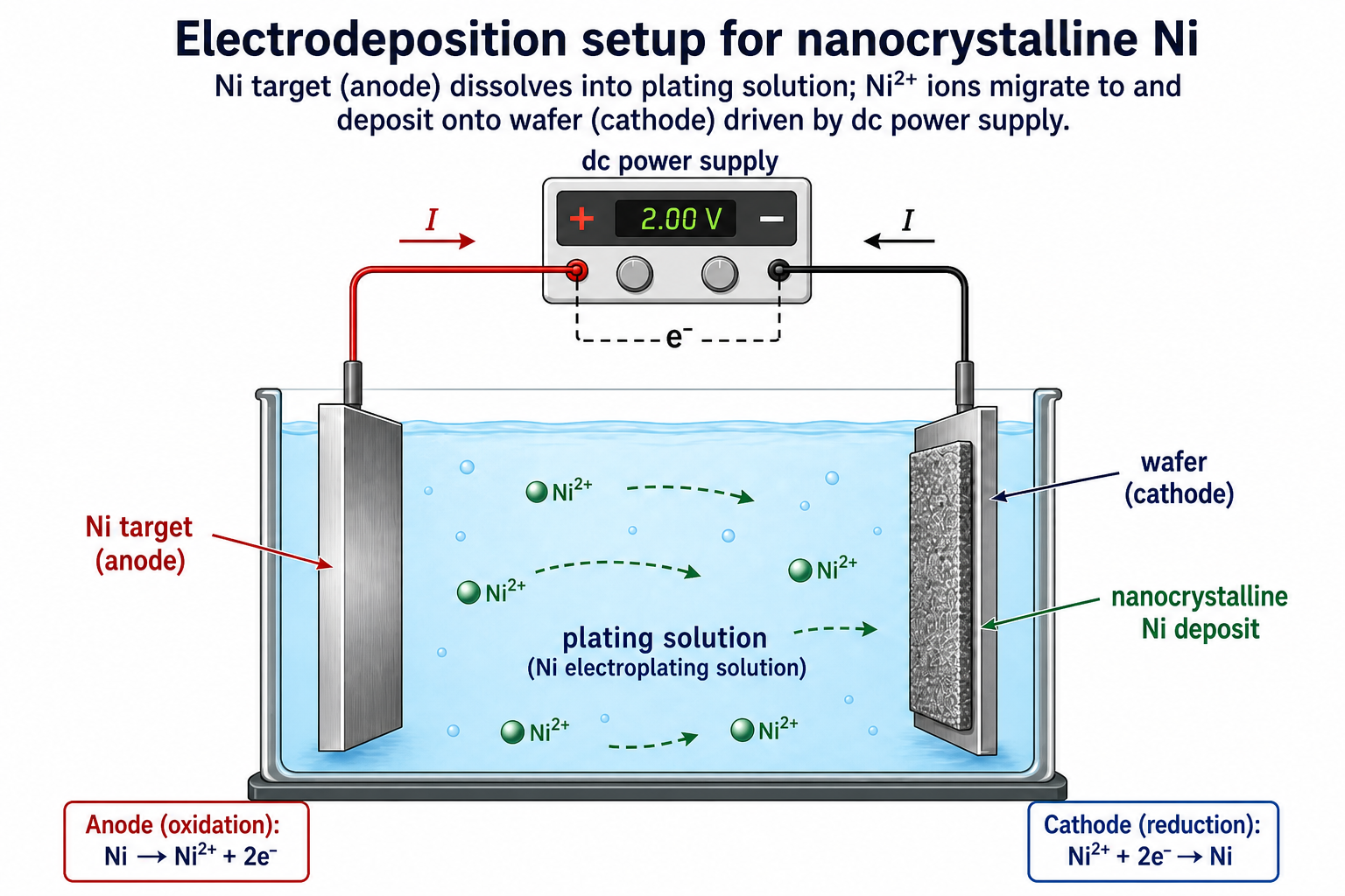
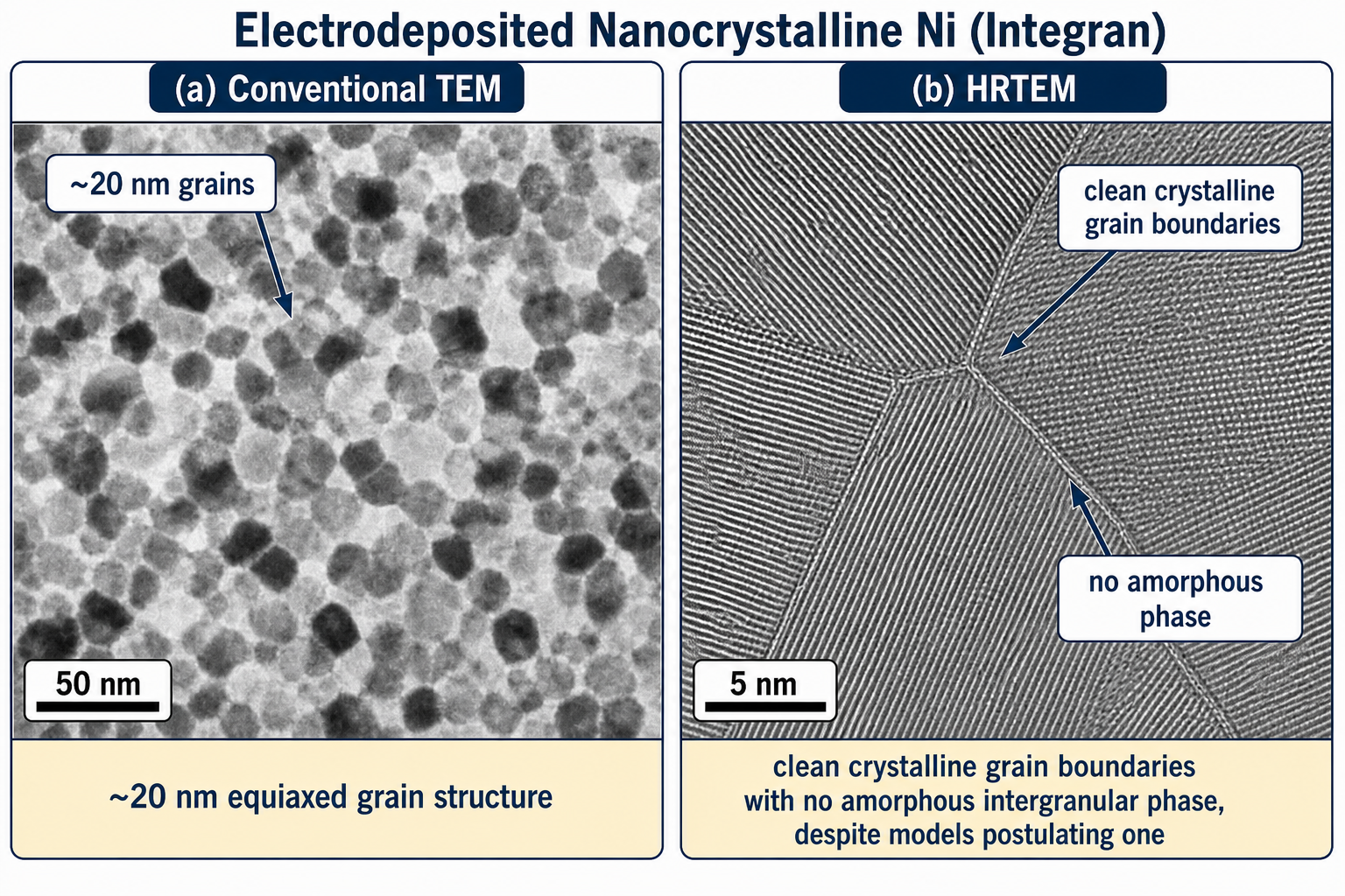
A critical refinement of the electrodeposition technique is pulse electrodeposition, in which the applied current alternates between on (deposition) and off (rest) cycles rather than flowing continuously. During each current-on pulse, a burst of new crystal nuclei forms on the cathode surface. During the off period, the ion-depleted diffusion layer near the cathode replenishes. Because each successive pulse nucleates fresh grains rather than simply growing the grains formed by the previous pulse, the average grain size can be driven far below what continuous DC deposition achieves. By optimising the pulse-on time (typically 1–10 ms), pulse-off time (10–100 ms), peak current density, and bath additives (grain refiners such as saccharin), nanocrystalline Ni with grain sizes below 20 nm has been routinely produced. The resulting material achieves Vickers hardness values exceeding 600 HV — comparable to many hardened steels — while retaining the ductility and corrosion resistance of pure nickel. Pulse electrodeposition is now used industrially for wear-resistant coatings, MEMS components, and electroformed moulds.
6 Powder Consolidation for Bulk Nanomaterials
Consolidation of nanocrystalline powders into bulk compacts involves four typical steps: (1) mixing of powders, (2) initial consolidation to form a green body, (3) further densification of the green body, and (4) finish machining. The central challenge is achieving full density while preventing grain coarsening.
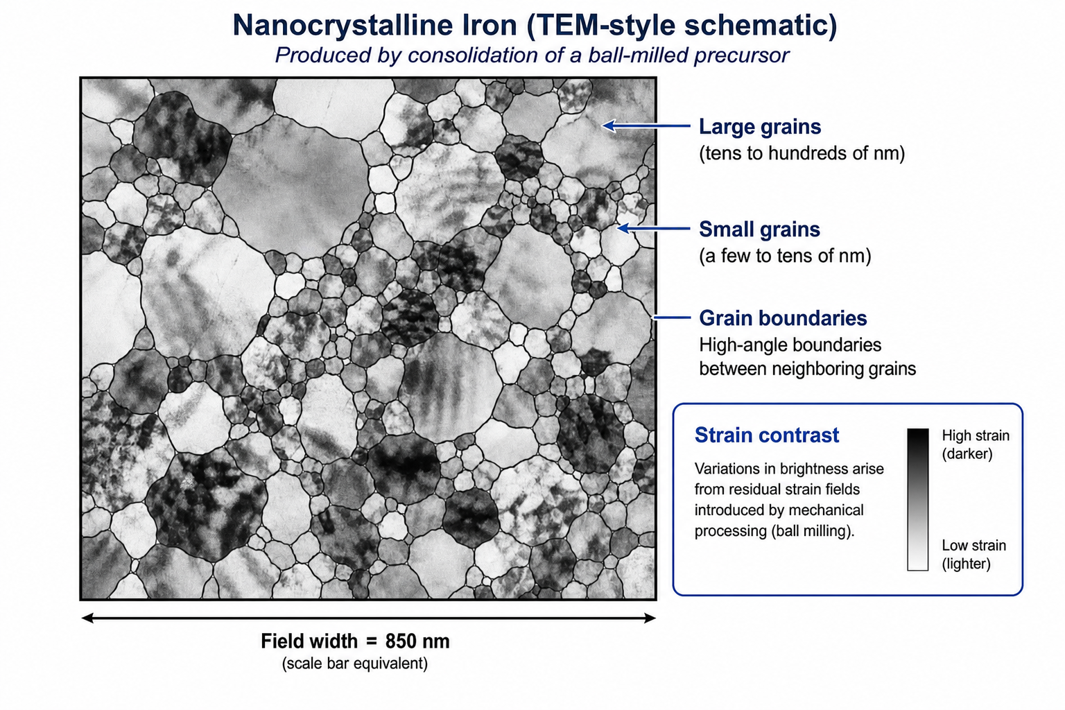
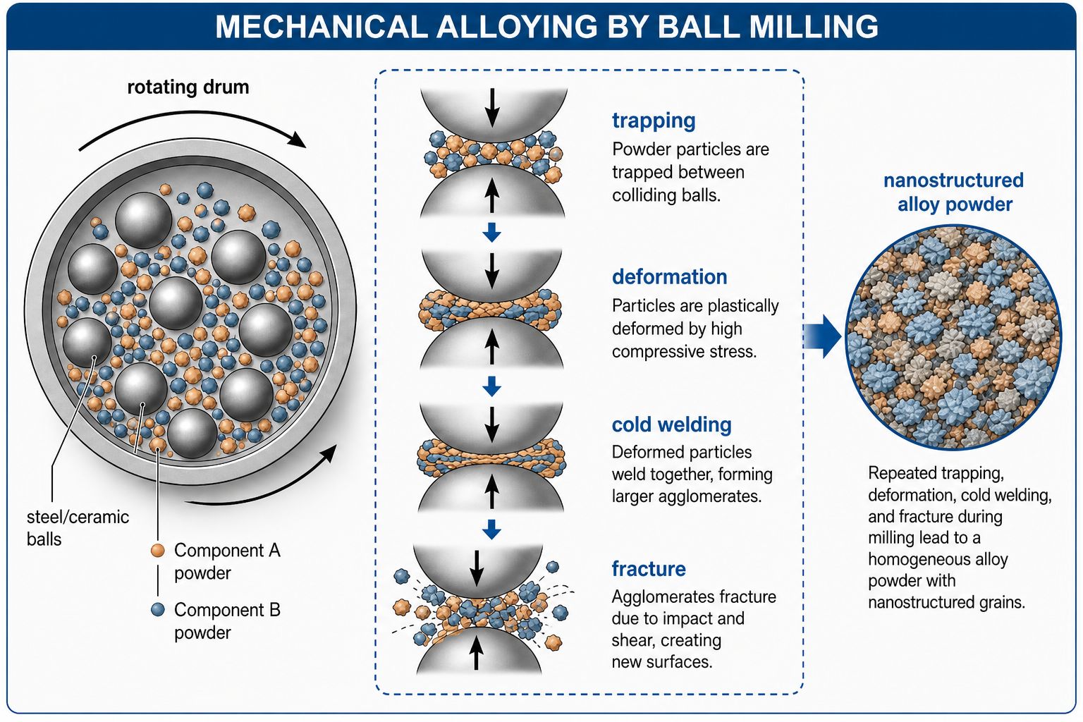
7 Pressure Sintering and Spark Plasma Sintering (SPS)
Pressure sintering is the standard consolidation route for nanopowders: simultaneous application of uniaxial pressure and heat in a heated die drives densification. The key challenge is that the temperatures needed for sintering also promote grain coarsening.
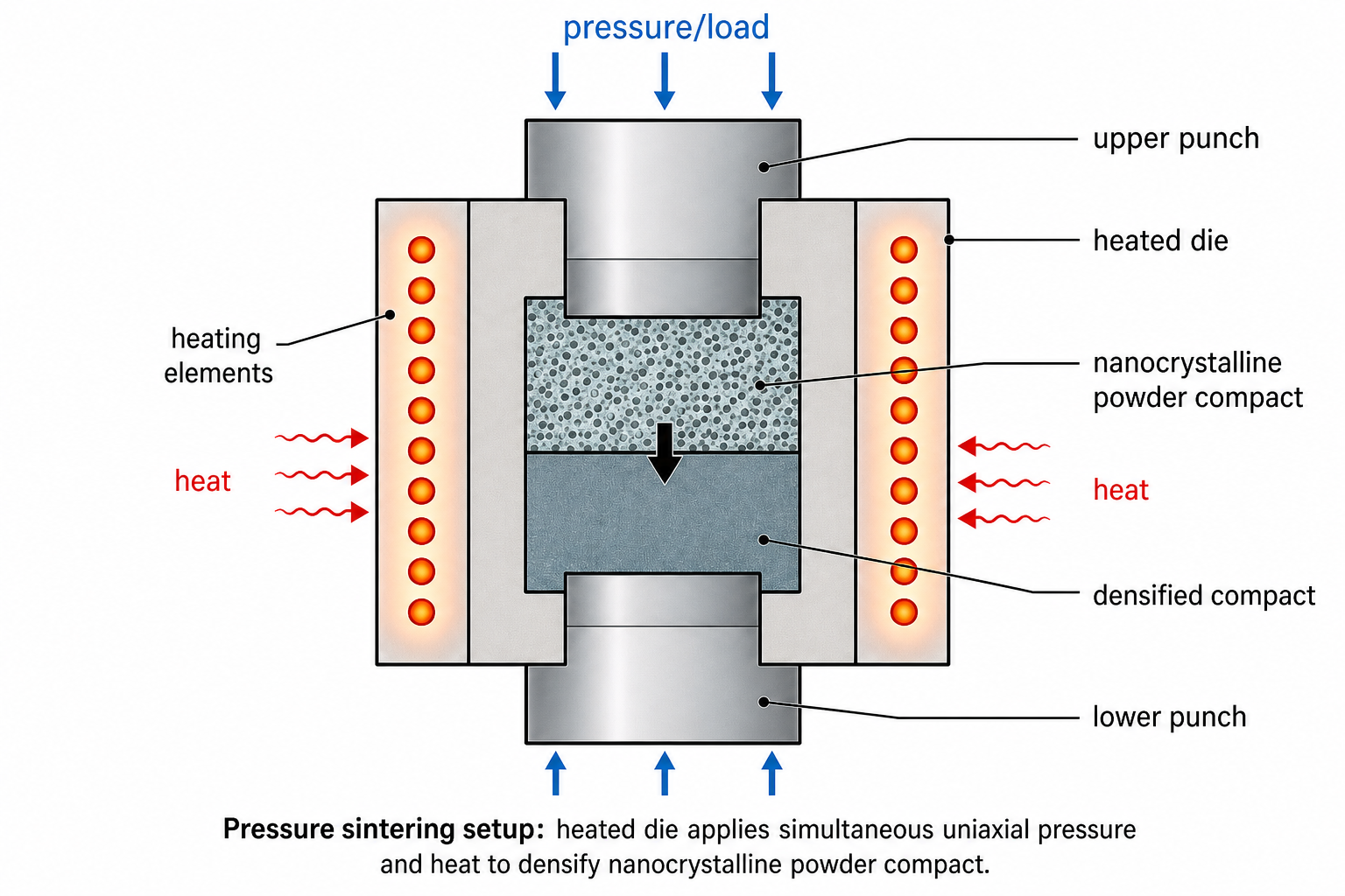
SPS combines pressure with rapid heating rates and pulsed direct current (PDC) passing through the electrically conducting graphite die. This "flash" or electric discharge sintering achieves very high heating rates, allowing compacts to be prepared at lower temperatures and shorter sintering times than conventional pressure sintering. The result is high sintering speed + low sintering temperature = small retained grain size.
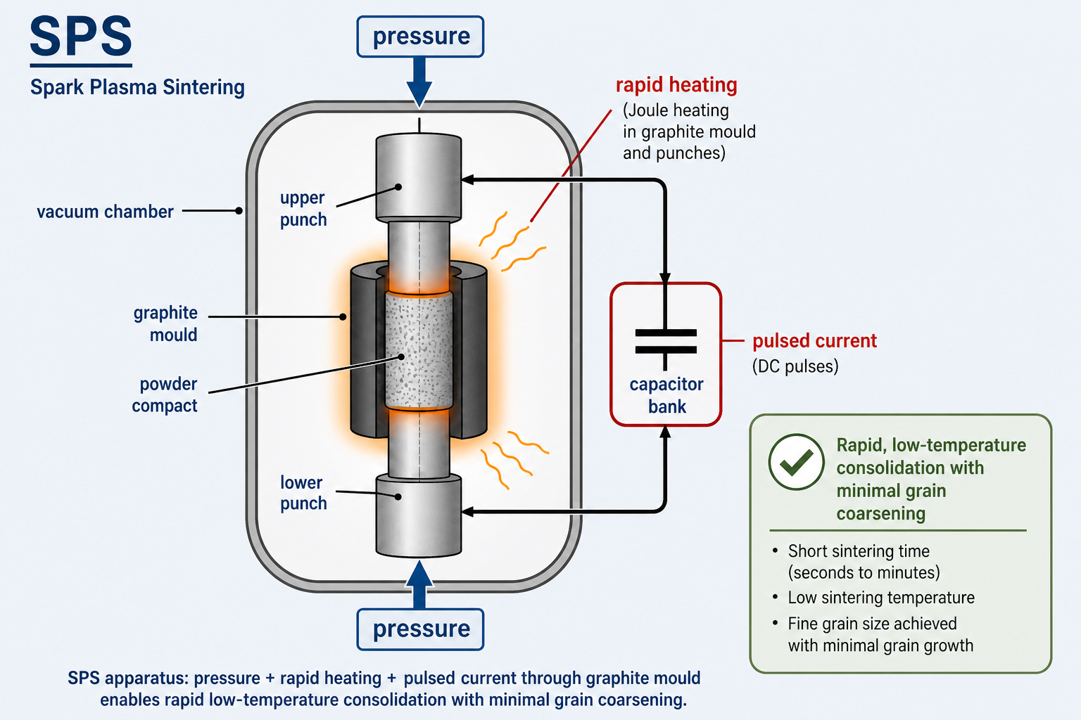
Three factors contribute to SPS densification: (i) mechanical pressure — removes pores by forcing particle contact; (ii) rapid heating rates — minimize time spent at elevated temperatures, limiting grain growth; (iii) pulsed direct current — generates Joule heating at particle contacts and subjects the compact to an electric field, potentially activating additional surface diffusion pathways.
8 Severe Plastic Deformation (SPD)
Severe Plastic Deformation (SPD) is a top-down approach that first develops very large plastic strains and then exploits recovery, recrystallization, and microstructural rearrangement to refine grains to the nanoscale. Recovery involves thermally enhanced dislocation motion to reduce internal stresses; recrystallization involves growth of nearly strain-free crystals; through rearrangement and annihilation of dislocations, a refined grain structure emerges.
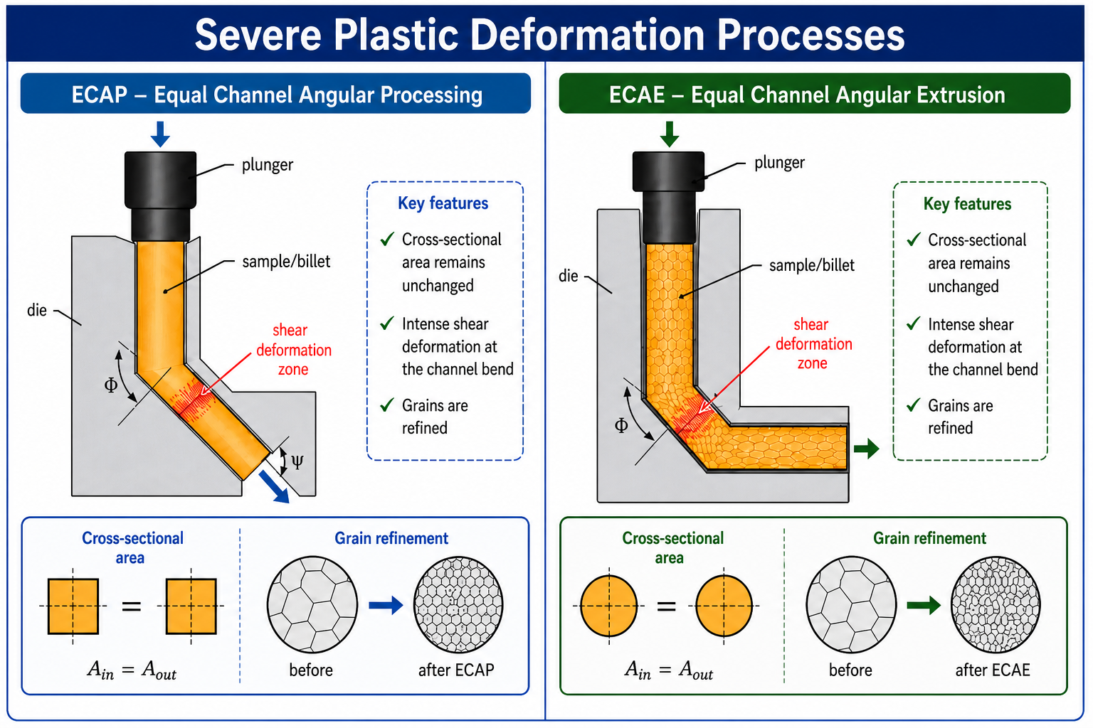
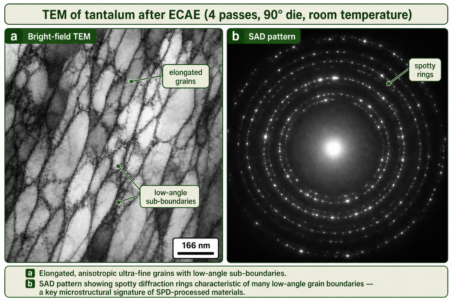
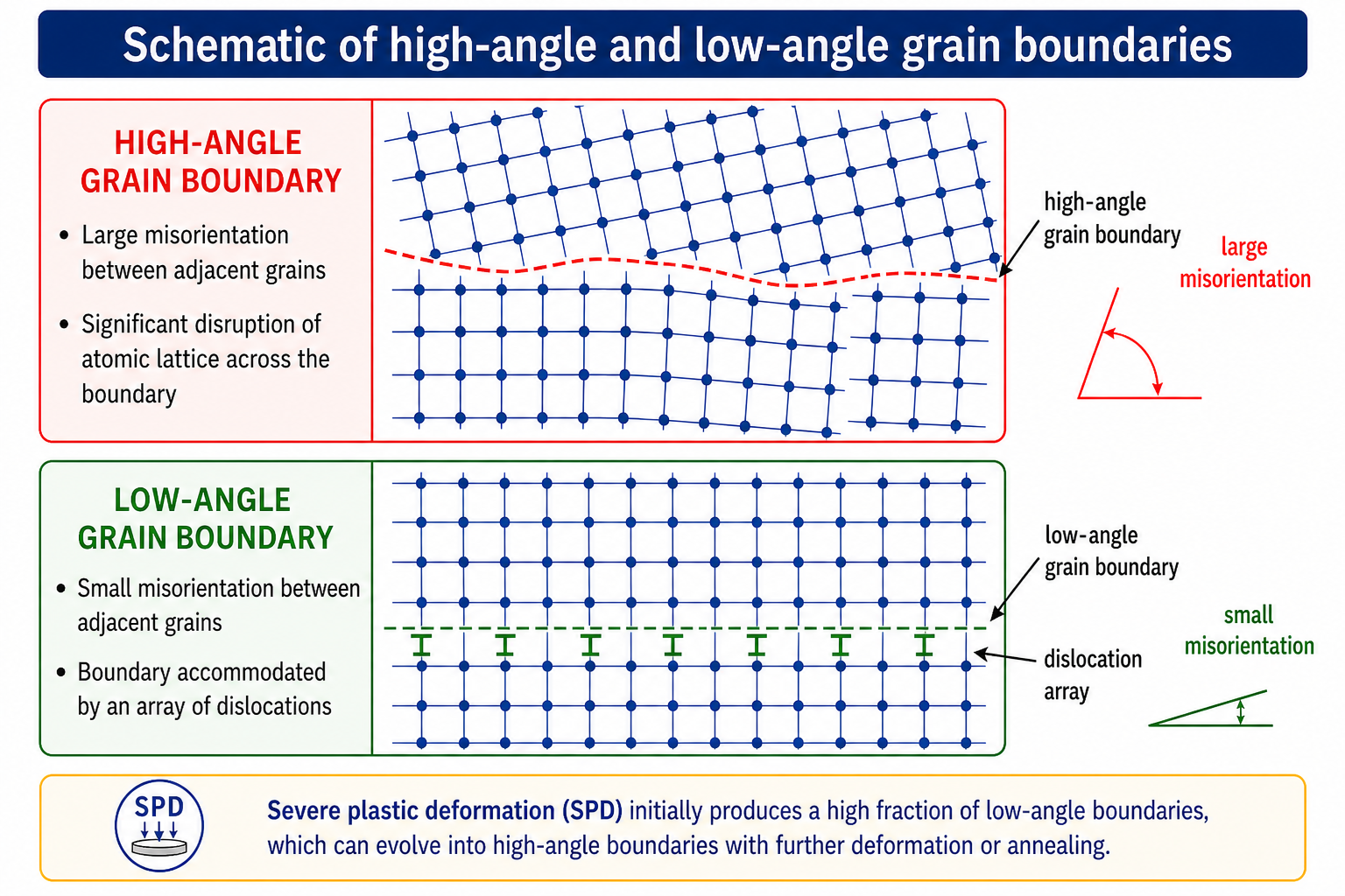
Beyond ECAP and ECAE, several other SPD techniques have been developed, each offering different trade-offs between achievable strain, specimen geometry, and scalability. High-Pressure Torsion (HPT) subjects a thin disc to simultaneous high compressive pressure and torsional shear between two anvils; the shear strain increases linearly with radial distance from the disc centre, and at the rim can exceed 100 after multiple turns. HPT produces the smallest grain sizes of any SPD method — routinely below 100 nm and in some systems approaching ~10 nm — but is limited to small disc specimens (~10 mm diameter, ~1 mm thick) and produces an inherently inhomogeneous microstructure. Accumulative Roll Bonding (ARB) is a scalable sheet-processing variant in which a metal sheet is cut in half, the halves are stacked, surface-cleaned, and roll-bonded together in a single pass; the cycle is repeated multiple times, each pass introducing a shear strain of ~0.8. After 6–8 ARB cycles, grain sizes of 100–500 nm are achieved in aluminium and copper alloys, and the process is compatible with existing industrial rolling infrastructure. Multi-Directional Forging (MDF) applies sequential compression along three orthogonal axes, rotating the workpiece 90° between each forging pass; the changing strain path promotes the formation of equiaxed, high-angle grain boundaries and avoids the elongated grain morphologies typical of unidirectional deformation. MDF is particularly useful for processing bulk billets of difficult-to-deform materials such as titanium and magnesium alloys.
Key Takeaways
- Sputtering outperforms evaporation for adhesion and multicomponent targets; evaporation gives larger grains and operates at much lower pressure.
- Dip coating film thickness is set by viscous drag vs. gravity; spin coating by centrifugal force and viscosity. Both suffer cracking risk from gel shrinkage stresses.
- Electrodeposition can produce fully dense nanocrystalline metals (e.g. Ni, ~20 nm grain size) with clean grain boundaries — no amorphous intergranular phase.
- Powder consolidation route: mix → green body → sintering → machining. Grain coarsening during sintering is the key challenge.
- SPS (pressure + rapid heating + pulsed current) achieves densification at lower temperatures and times, preserving nanoscale grain size.
- SPD (ECAP/ECAE) introduces severe shear without changing cross-section, refining grains via recovery and recrystallization; initially produces many low-angle grain boundaries.
- G. Cao, Nanostructures and Nanomaterials: Synthesis, Properties and Applications, Imperial College Press, 2004.
- C. Suryanarayana, "Mechanical Alloying and Milling," Progress in Materials Science, 46, 1–184, 2001.
- R.Z. Valiev & T.G. Langdon, "Principles of Equal-Channel Angular Pressing as a Processing Tool for Grain Refinement," Progress in Materials Science, 51, 881–981, 2006.
Mechanical Properties of Nanomaterials
High-Pressure Torsion as a severe plastic deformation route, scale-dependence of mechanical properties, grain boundary strengthening mechanisms, the Hall–Petch relation and its breakdown at nanoscale grain sizes, and the extraordinary strength of nanolaminates.
Contents
1 High-Pressure Torsion (HPT)
High-Pressure Torsion is the third major severe plastic deformation (SPD) process alongside ECAP and ECAE. A thin disc-shaped specimen — typically 10 mm in diameter and 1 mm thick — is placed between two anvils. A large compressive pressure is applied and one anvil is rotated, subjecting the disc to simultaneous high pressure and intense torsional shear. The shear strain introduced is given by:
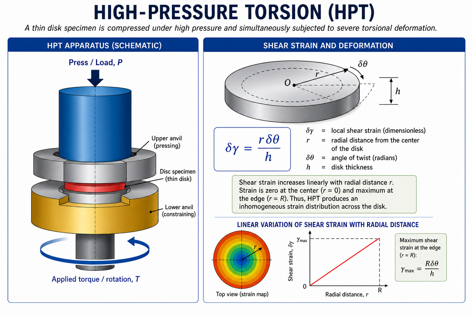
Despite achieving extremely large strains, HPT has three significant limitations: (i) the superimposed pressure is necessary to prevent the specimen from fracturing, yet workability issues often still require elevated-temperature processing; (ii) the specimen size is inherently small (~1 cm diameter), limiting the quantity of material produced; and (iii) strain is highly inhomogeneous — the centre of the disc experiences near-zero strain while the rim experiences the maximum. HPT is therefore not a viable route for producing significant quantities of bulk nanomaterial.
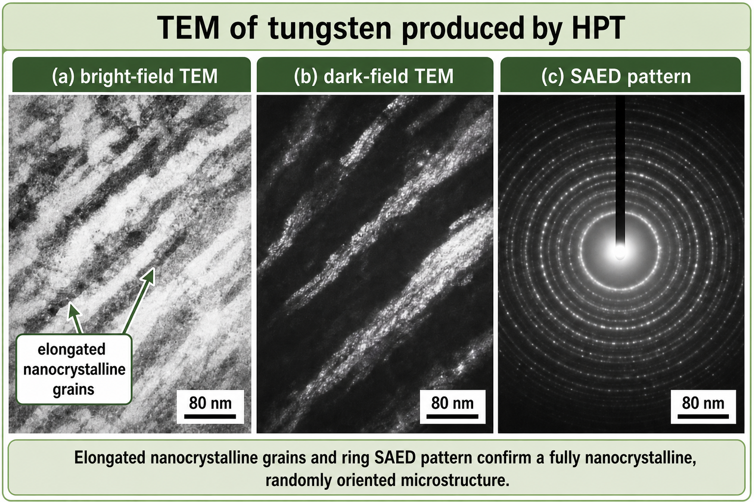
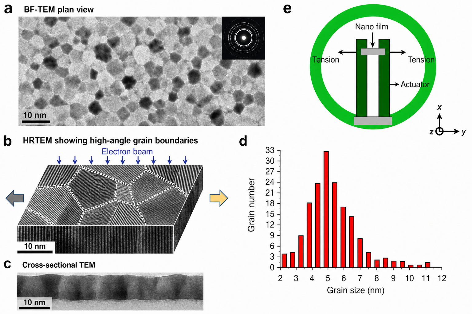
2 Grain Boundary Volume Fraction & Material Extremes
In a conventional polycrystalline material, grain size is typically between 0.1 mm and 1 mm. The disordered grain boundary region — roughly two to three atomic layers wide — represents only a tiny fraction of the total volume, perhaps one part in a million. In nanocrystalline materials with grain sizes of 10–100 nm, the same grain boundary width now constitutes a substantial fraction of the total volume. This dramatic increase in the disordered boundary volume fraction is the root cause of the unique properties of nanomaterials.
As grain size shrinks toward atomic dimensions, the material approaches total disorder throughout its volume. The amorphous state represents the limiting case of a nanostructured material — a crystal with grain size of one atom — and one might expect its properties to represent extremes as well.
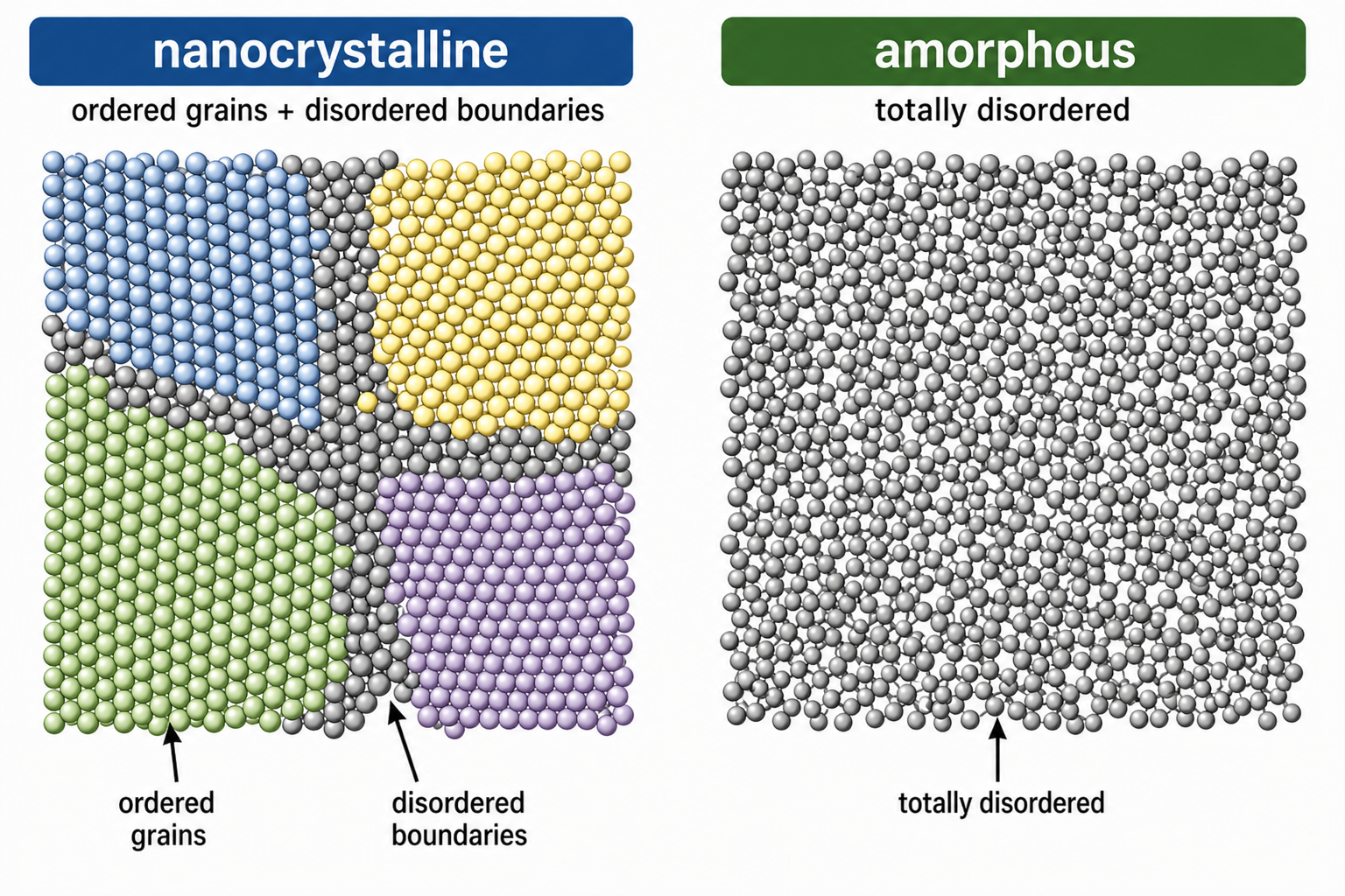
3 Scale Dependence of Properties & Nanodispersion Hardening
The bulk properties of conventional materials — density, elastic modulus, yield strength, thermal and electrical conductivity — are intrinsic and scale-independent. A small piece of steel has the same Young's modulus as a large piece. This is the foundational assumption of continuum mechanics and greatly simplifies structural analysis. However, the continuum approximation breaks down at the nanoscale, and the exceptions have given rise to some of the strongest and most useful materials we have.
A prime and historically important example is nanodispersion hardening — specifically precipitation hardening of aluminium alloys. The Al-4%Cu system illustrates the principle clearly. When heated to 550°C, Cu dissolves fully into the Al matrix; rapid quenching retains Cu in supersaturated solid solution, slightly distorting the Al crystal lattice. Subsequent ageing at 150°C drives diffusion-controlled precipitation of Cu as nanoscale CuAl₂ particles — needle-like platelets approximately 2 nm wide and 30 nm long, spaced about 30 nm apart.
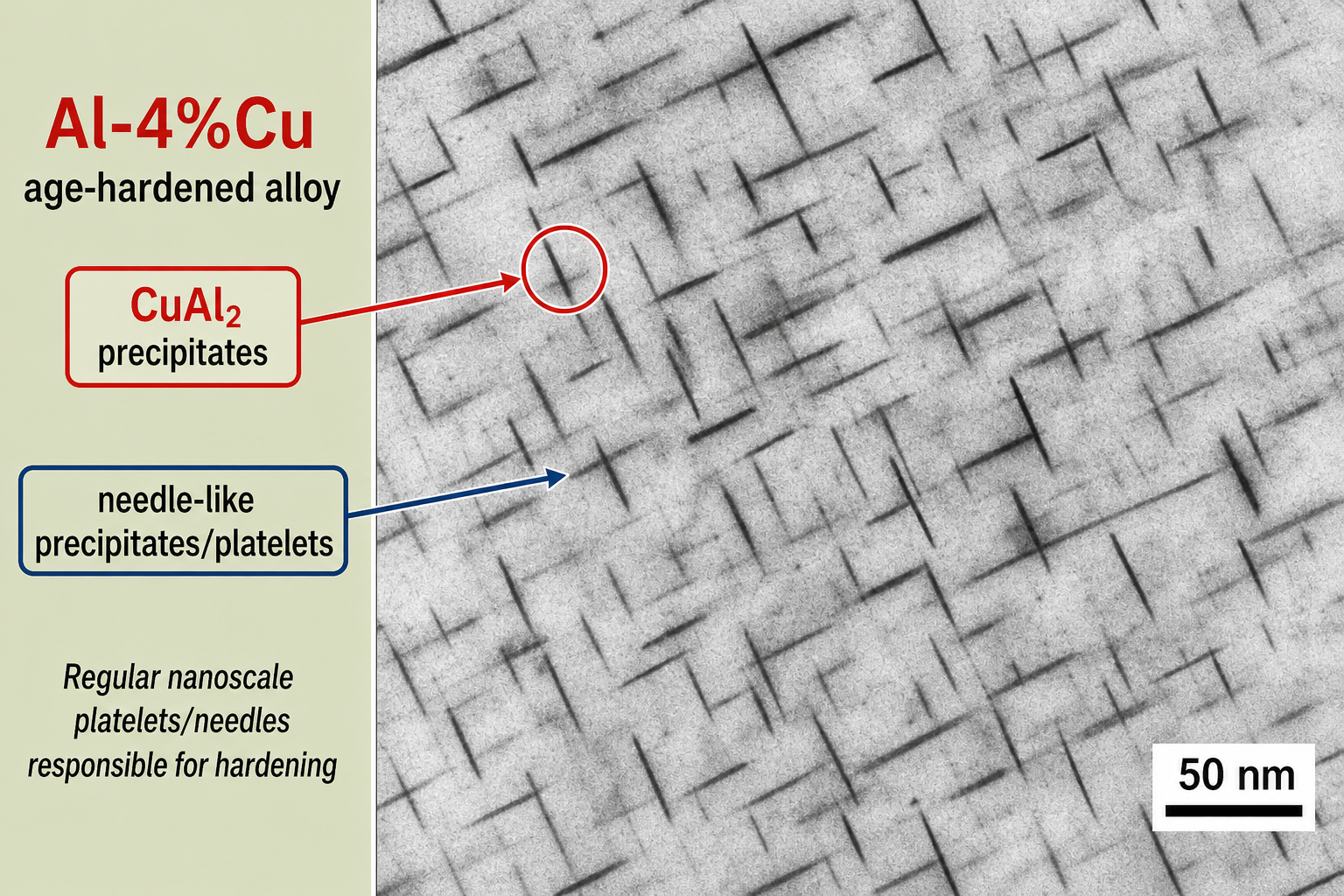
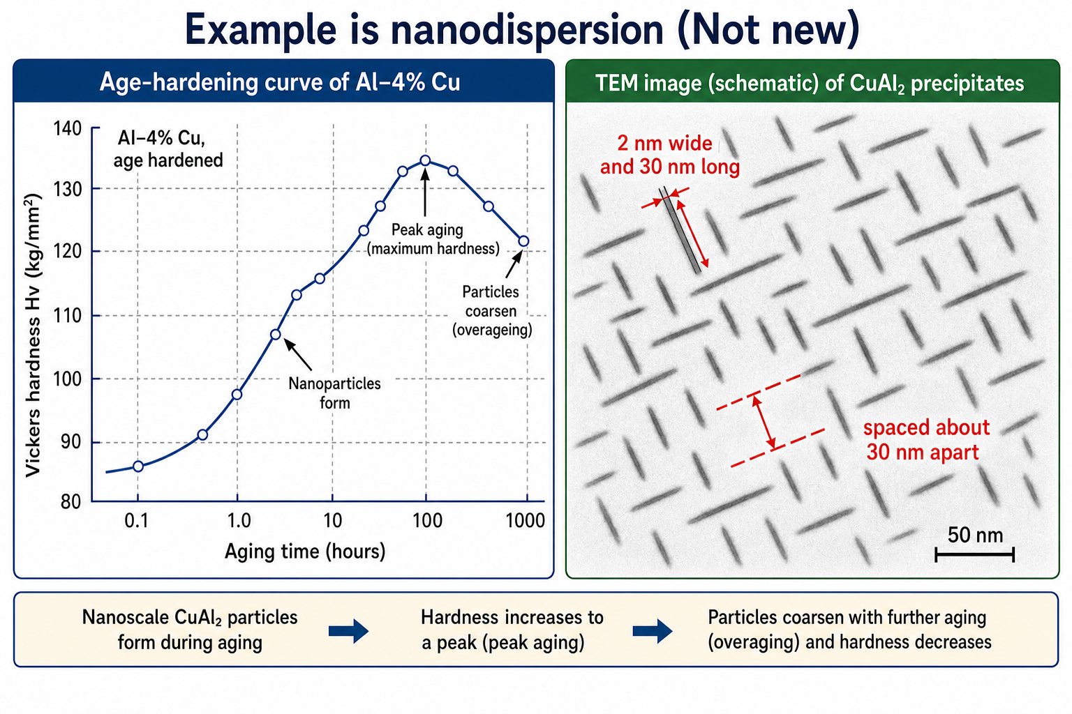
Most high-strength aluminium, magnesium, titanium, and steel alloys in use today — and for many decades — derive their strength from nanoscale microstructural features. Age-hardening of aluminium alloys was discovered empirically by Alfred Wilm in 1906, decades before the concept of "nanotechnology" existed. The underlying mechanism — nanoscale precipitate particles blocking dislocation motion — is a nanoscale phenomenon that has been exploited industrially for over a century.
4 Dislocation Obstacles & Strengthening Mechanisms
Three classical mechanisms operate to strengthen metals by impeding dislocation motion. All three become dramatically more effective when their characteristic spacing is reduced to the nanoscale:
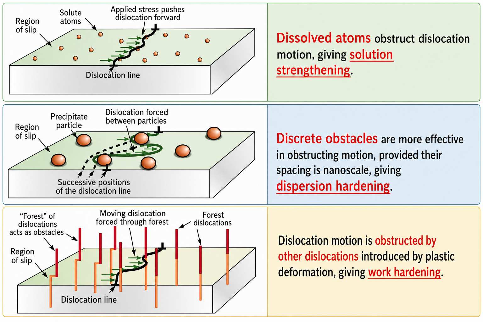
5 Hall–Petch Relation & Its Breakdown
Grain boundaries act as obstacles to dislocation motion for two reasons: the boundary region is locally disordered, and the slip planes in adjacent grains are not coplanar. The "strength" of a boundary as an obstacle is quantified by the critical force per unit dislocation length, f*, required to transmit slip across it. Dislocations pile up at boundaries until the stress on the lead dislocation exceeds f*, at which point slip propagates into the next grain.
This pileup mechanism leads to the Hall–Petch relationship: strength (or hardness) increases as grain size decreases, scaling as d−½. Coarse-grained copper (grain size ~50 mm) has a hardness below 200 MPa; reducing grain size to 5 nm raises hardness to over 2000 MPa — more than a factor of ten increase.
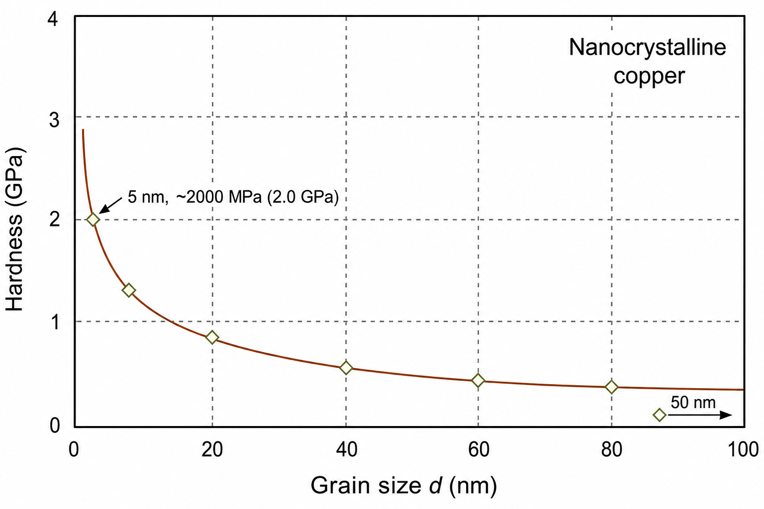
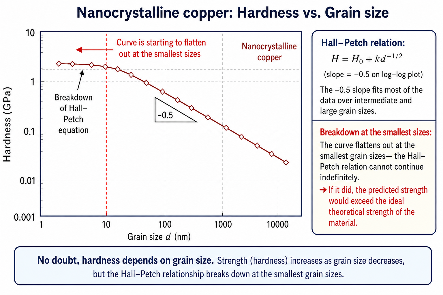
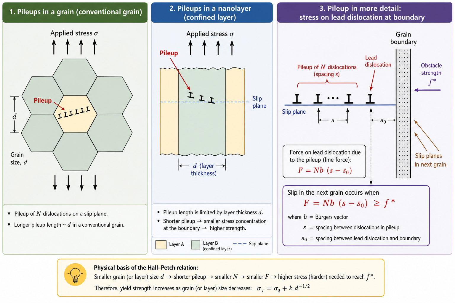
The Hall–Petch relation holds as long as a grain is large enough to contain a pileup of multiple dislocations. Once grain size falls to ~10–20 nm, only one or two dislocations can fit in a grain — there is no pileup. Beyond this point, other deformation mechanisms (grain boundary sliding, diffusional creep) take over and the Hall–Petch slope breaks down or even reverses (the "inverse Hall–Petch" effect).
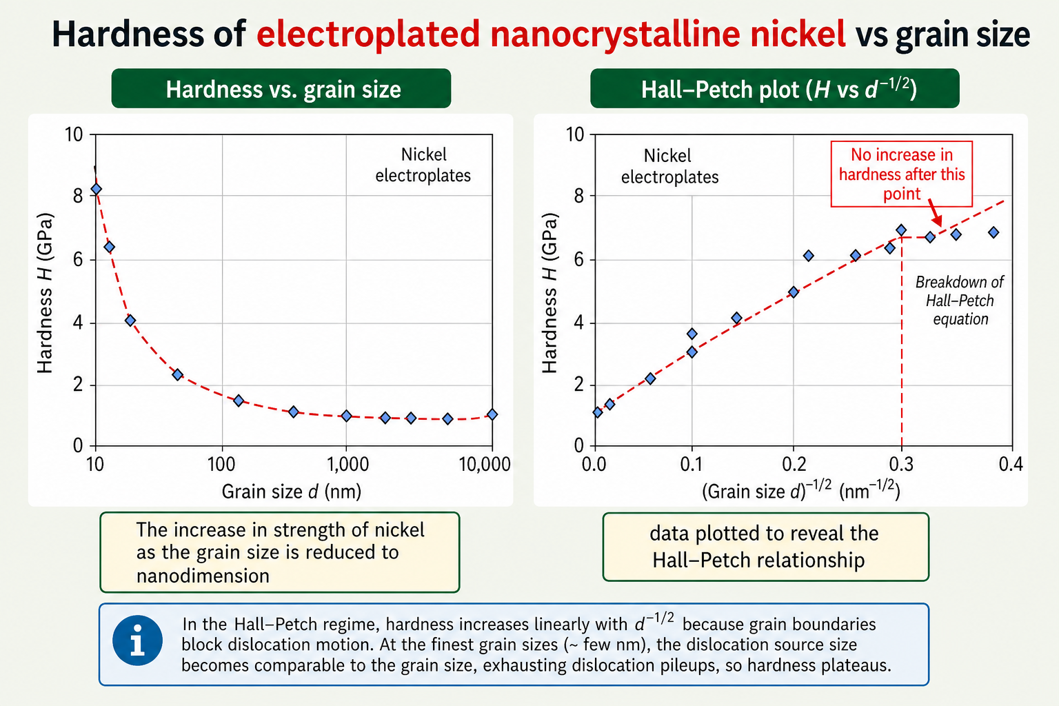
6 Nanolaminates
Nanolaminates are multilayer thin film structures composed of alternating layers of two different materials, each layer typically between a few atomic layers and a few tens of nanometres thick. They are produced by sequential evaporation or sputtering from two separate sources. The bilayer period d — the combined thickness of one pair of layers — plays the same role as grain size in the Hall–Petch analysis: dislocations pile up against the interfaces, and strength increases as d decreases.
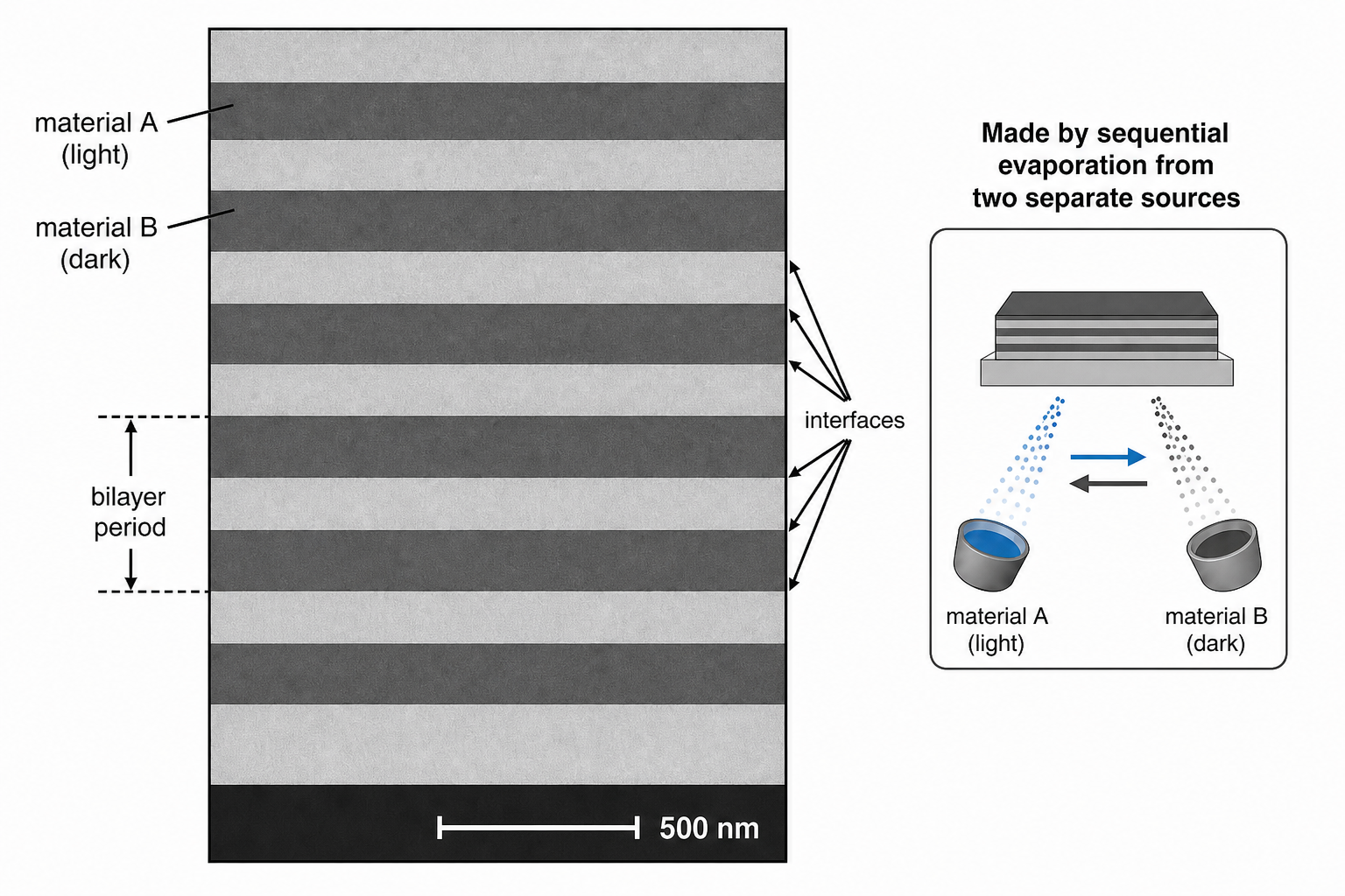
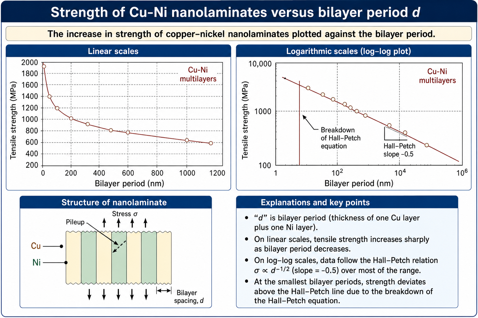
The microstructure of thin films — whether produced by sputtering, evaporation, or CVD — is governed at the earliest stages by the nucleation mode, which in turn is controlled by the relative surface energies of the film, the substrate, and the film-substrate interface. Three classical modes are recognised. In Volmer-Weber (island) growth, the film material has a high contact angle on the substrate — atoms arriving on the surface bond more strongly to each other than to the substrate, so they cluster into discrete three-dimensional islands that eventually coalesce. This mode is typical of metals deposited on oxides. In Frank-van der Merwe (layer-by-layer) growth, the film wets the substrate completely — the surface energy of the film is lower than that of the substrate, so each monolayer is completed before the next begins. This is the mode exploited in MBE growth of lattice-matched semiconductor heterostructures. In Stranski-Krastanov (layer-plus-island) growth, the first few monolayers grow layer-by-layer, but as the film thickens, accumulated lattice mismatch strain raises the elastic energy until it becomes energetically favourable to relax that strain by forming three-dimensional islands on top of the wetting layer. This strain-driven transition is the basis of quantum dot self-assembly — InAs islands on GaAs, for example, spontaneously form size-uniform quantum dots in the 5–20 nm range without any lithographic patterning.
Beyond the initial nucleation mode, the overall film microstructure that develops during continued deposition is well described by zone models. The Movchan-Demchishin model (1969) and the later Thornton model (1974) classify film structure as a function of the homologous temperature T/Tm (substrate temperature divided by the melting point of the film material). Zone 1 (T/Tm < 0.3) produces tapered columnar grains separated by open voided boundaries — surface diffusion is negligible, so atoms stick where they land, and shadowing by surface roughness creates porous, low-density films. Zone T (the transition zone, T/Tm ≈ 0.3–0.5) produces dense, fibrous columnar grains with competitive growth — surface diffusion is active enough to fill voids but not to produce well-defined faceted grains. Zone 2 (T/Tm ≈ 0.5–0.7) produces well-defined columnar grains whose width increases with film thickness, driven by surface-diffusion-controlled grain boundary migration. Zone 3 (T/Tm > 0.7) produces equiaxed grains formed by bulk diffusion and recrystallisation — the film structure resembles a bulk annealed polycrystal. Thornton extended the model by adding a second axis for sputtering gas pressure, showing that higher Ar pressure (more gas-phase scattering, lower adatom energy) shifts the structure toward Zone 1 even at higher temperatures. These zone models are essential for predicting and controlling film properties: Zone 1 films are porous and soft; Zone T and Zone 2 films are dense and hard; Zone 3 films are ductile but may be too coarse-grained for nanoscale applications.
All thin films deposited on substrates develop residual stress, which profoundly affects their mechanical integrity, adhesion, and functional properties. The total stress has two components. Intrinsic stress arises from the growth process itself: tensile intrinsic stress develops when atoms deposited at low mobility leave voids or incomplete grain boundaries that tend to contract (grain boundary relaxation); compressive intrinsic stress develops when energetic arriving atoms (as in magnetron sputtering or ion-assisted deposition) are implanted into subsurface sites, creating an excess atomic density — a process termed atomic peening. Thermal stress arises on cooling from the deposition temperature due to the difference in coefficient of thermal expansion (CTE) between the film and substrate: σthermal = Ef(αs − αf)ΔT / (1 − νf), where Ef is the film modulus, α values are the CTEs, and ΔT is the temperature drop. When the total stress exceeds a critical threshold, the film may crack (tensile failure), buckle and delaminate (compressive failure), or — in carefully engineered systems — exploit stress intentionally. For example, the compressive strain in a thin Ge layer on Si can drive Stranski-Krastanov island formation, producing self-assembled quantum dots whose size and spacing are tuned by the magnitude of the lattice mismatch strain.
Key Takeaways
- HPT applies simultaneous high pressure and torsional shear to produce nanocrystalline discs (~10 mm, ~1 mm thick); strain is inhomogeneous and specimen size is small — not scalable for bulk production.
- Grain boundary volume fraction increases dramatically as grain size enters the nanometre range, driving unique mechanical properties.
- The amorphous state is the limiting case of a nanostructured material — grain size of atomic dimensions, total disorder.
- Three dislocation strengthening mechanisms — solution strengthening, dispersion hardening, work hardening — all become more effective at nanoscale feature spacings.
- The Hall–Petch relation (strength ∝ d−½) predicts hardness increasing with decreasing grain size; coarse Cu (~200 MPa) vs nanocrystalline Cu at 5 nm (~2000 MPa).
- Hall–Petch breaks down below ~10–20 nm when grains are too small to sustain dislocation pileups; other mechanisms take over.
- Nanolaminates show identical Hall–Petch strengthening controlled by bilayer period rather than grain size, with the same slope and the same breakdown at small periods.
- M.F. Ashby et al., Nanomaterials, Nanotechnologies and Design, Butterworth-Heinemann, 2009.
- R.Z. Valiev & T.G. Langdon, "Principles of Equal-Channel Angular Pressing as a Processing Tool for Grain Refinement," Progress in Materials Science, 51, 881–981, 2006.
- D. Jang et al., "Deformation mechanisms in nanocrystalline metals," Nature Communications, 5, 4402, 2014. doi:10.1038/ncomms5402
Mechanical Limits & Thermal Properties of Nanomaterials
From the ideal strength ceiling and Ashby property charts to the thermodynamics of size-dependent melting — understanding why nanomaterials behave so differently from their bulk counterparts.
Contents
- Dislocation Motion, Pileups, and the Amorphous Extreme
- Ashby Charts for Nanomaterials: Yield and Tensile Strength vs Density
- The Ideal Strength: A Fundamental Ceiling
- Thermal Properties: Why Melting Point Is Size-Dependent
- Thermodynamic Derivation of Size-Dependent Melting
- The Size-Dependent Melting Point Formula
- Experimental Evidence: Melting Point vs Particle Size
1 Dislocation Motion, Pileups, and the Amorphous Extreme
Plastic deformation in a crystalline material requires dislocations to sweep across slip planes and penetrate grain boundaries or layer interfaces as they do so. The critical variable is the grain size d. When d is large, many dislocations can queue behind one another at a boundary, forming an extended pileup that concentrates stress and eventually forces slip into the neighbouring grain at a relatively modest applied stress — hence relatively modest strength. As d shrinks into the nanometre regime, the number of dislocations that can be accommodated in any single pileup diminishes rapidly, and the stress required to propagate deformation rises in proportion. This is the Hall–Petch mechanism in its most direct physical reading: fewer dislocations per pileup, higher effective barrier, greater strength.
Carried to its logical extreme, grain refinement reaches a point at which the crystal size itself becomes comparable to atomic dimensions. At this scale the material is no longer meaningfully crystalline — it becomes structurally completely disordered, i.e. amorphous. In an amorphous metal, dislocations as well-defined line defects cease to exist. Instead, plastic flow must proceed by shear-transformation-zone activation in the disordered matrix, a process that requires overcoming a much higher local energy barrier. Dislocations do interact strongly with the disordered regions they encounter even in partially nanocrystalline materials, and in fully amorphous metals this interaction governs the entire deformation response — giving amorphous metals their characteristically high hardness and strength.
The progression from coarse-grained → nanocrystalline → amorphous represents a continuum of increasing structural disorder. Mechanical strength rises progressively along this continuum, ultimately because dislocation glide — the easiest mode of plasticity in crystalline solids — becomes either severely restricted or entirely suppressed.
2 Ashby Charts for Nanomaterials: Yield and Tensile Strength vs Density
Ashby property charts plot one material property against another on logarithmic axes, grouping classes of materials into characteristic bubbles. When nanomaterials are added to the classic yield strength–density chart, the picture changes strikingly. Nanocrystalline metals occupy a field shifted substantially upward from their conventional coarse-grained counterparts, reflecting the Hall–Petch strengthening discussed above. Ceramic nanocomposites and metallic nanocomposites also push into high-strength territory. Most dramatic are nanowires of Cu, Ag, and Au, which approach strengths of tens of thousands of MPa at densities typical of these metals — a consequence of the near-elimination of dislocation sources in a thin wire geometry.
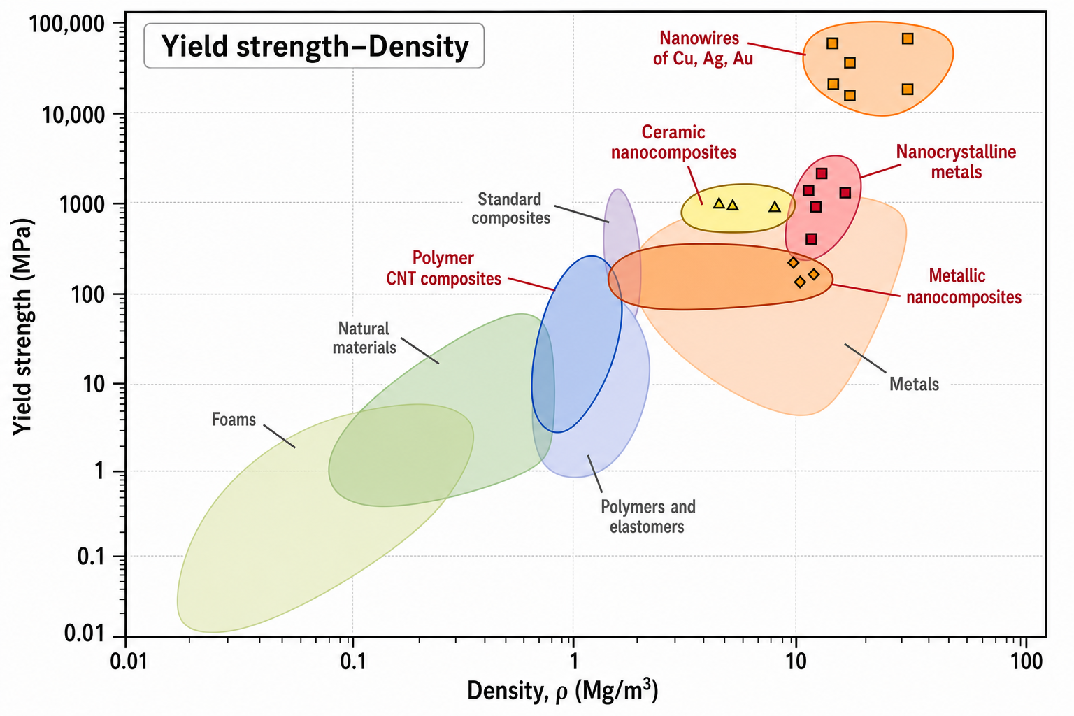
The tensile strength–density chart tells a similar but richer story, because it also distinguishes one-dimensional nanostructures. 1-D carbon nanostructures (carbon nanotubes) occupy an extraordinary position — tensile strengths in the range of hundreds of thousands of MPa at a density below 2 Mg/m³, far exceeding any bulk material. 1-D metallic nanostructures (metal nanowires) follow at somewhat lower strength. Three-dimensional ceramic nanocomposites, nanocrystalline metals, and metallic nanocomposites each define distinct high-performance bubbles, all displaced upward relative to conventional metals and ceramics.
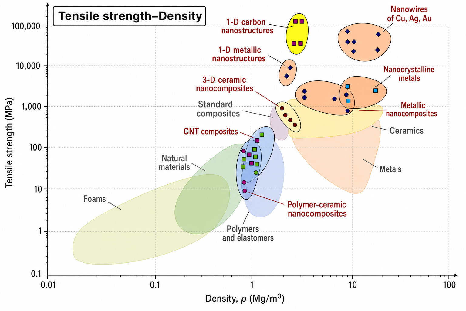
3 The Ideal Strength: A Fundamental Ceiling
Every strength value on an Ashby chart is bounded above by the theoretical or ideal strength of a material — the stress required to shear a perfect crystal across an atomic plane in the complete absence of defects. This ideal strength is typically of order E/10 to E/30, where E is Young's modulus. On the normalised chart plotting σy/E on the y-axis, the ideal strength appears as a horizontal band near 10−1.
Nano multilayers and amorphous metals cluster closest to this band among metallic materials — their strength-to-modulus ratios reach 10−1 to approaching 10−2, far above conventional Ti alloys, brass, mild steel, or aluminium alloys which sit at 10−3. Engineering polymers such as PTFE, PE, PS, PA, PET and PVC span a comparable normalised range by virtue of their low moduli. Ceramics such as zirconia and alumina also approach the ideal strength band. The instructive point is that nanostructured metals are genuinely approaching a physical limit — it will be very difficult to engineer materials stronger than this ceiling.
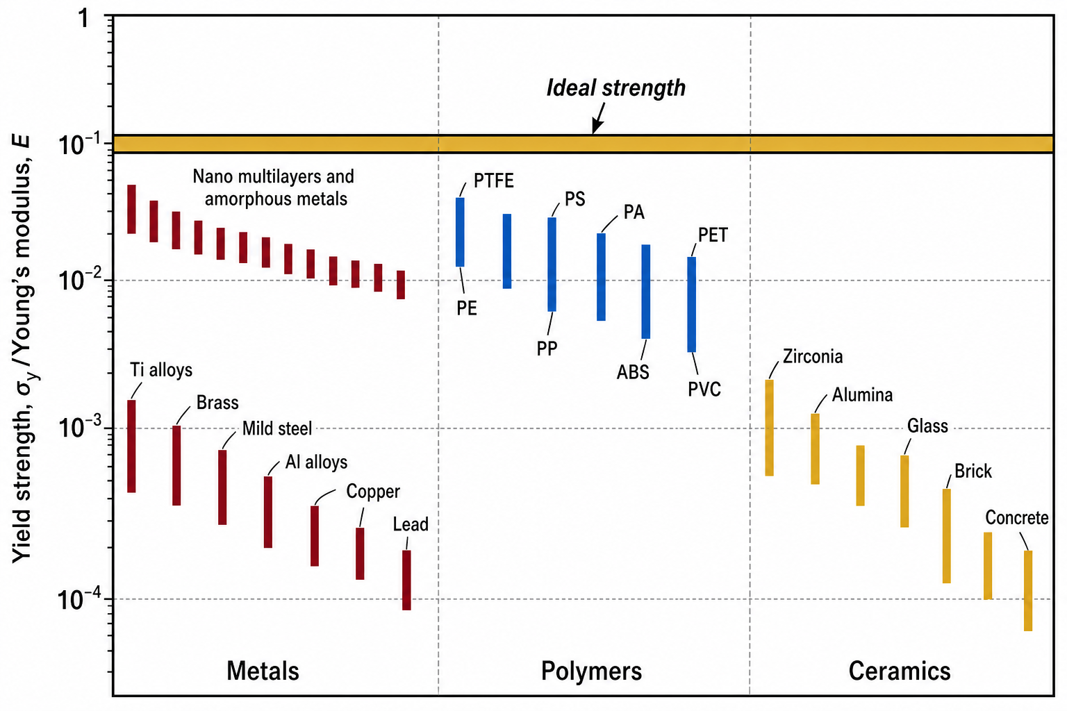
We are approaching an absolute upper bound on material strength. The ideal strength — of order E/10 — cannot be exceeded by any real material. Nano multilayers and amorphous metals are the closest any engineering metal has come to this ceiling, which is why it is very difficult to make materials stronger than these classes.
4 Thermal Properties: Why Melting Point Is Size-Dependent
The melting point of a material is one of its most fundamental properties — it directly reflects bond strength and therefore determines thermal stability, processing windows, and high-temperature performance. In a bulk solid, the surface-to-volume ratio is negligibly small and the curvature of any external surface is negligible. The thermodynamics of melting is therefore dominated by the bulk free energy change, and surface effects can be safely disregarded.
For nanoscale solids the situation is qualitatively different. The ratio of surface area to mass is large — for a 5 nm radius sphere, roughly 10% of atoms sit at or near the surface. For zero-dimensional (0-D) nanoparticles and one-dimensional (1-D) nanowires the surface curvature is pronounced. As a result, the system can no longer be treated as purely bulk; it must be regarded as containing both a volume phase and a surface phase. The thermodynamic consequence is that the melting temperature becomes size-dependent: it is no longer a fixed material constant but varies with particle radius.
To capture this correctly one must introduce an additional surface free energy term ΔGSurface into the total free energy change, so that:
ΔGTotal = ΔGBulk + ΔGSurface
where ΔGBulk is the classical bulk latent-heat term and ΔGSurface captures the additional contribution from creating and destroying surfaces during the solid → liquid transition.
5 Thermodynamic Derivation of Size-Dependent Melting
The bulk contribution to the free energy change on melting can be written in terms of the latent heat of melting Lo, the bulk melting temperature To, the actual (nanoscale) melting point T, and the volume of liquid VL formed:
ΔGBulk = [Lo(To − T) / To] × VL
When the surface area of the nanoparticle increases — as happens when a liquid layer nucleates on the solid surface — the change in surface energy is:
ΔGSurface = γ ΔA
where γ is the surface tension and ΔA is the increment in surface area. Physically, at the melting temperature a thin liquid layer of thickness t forms on the particle surface and advances inward at a certain rate — a process known as surface melting or premelting.
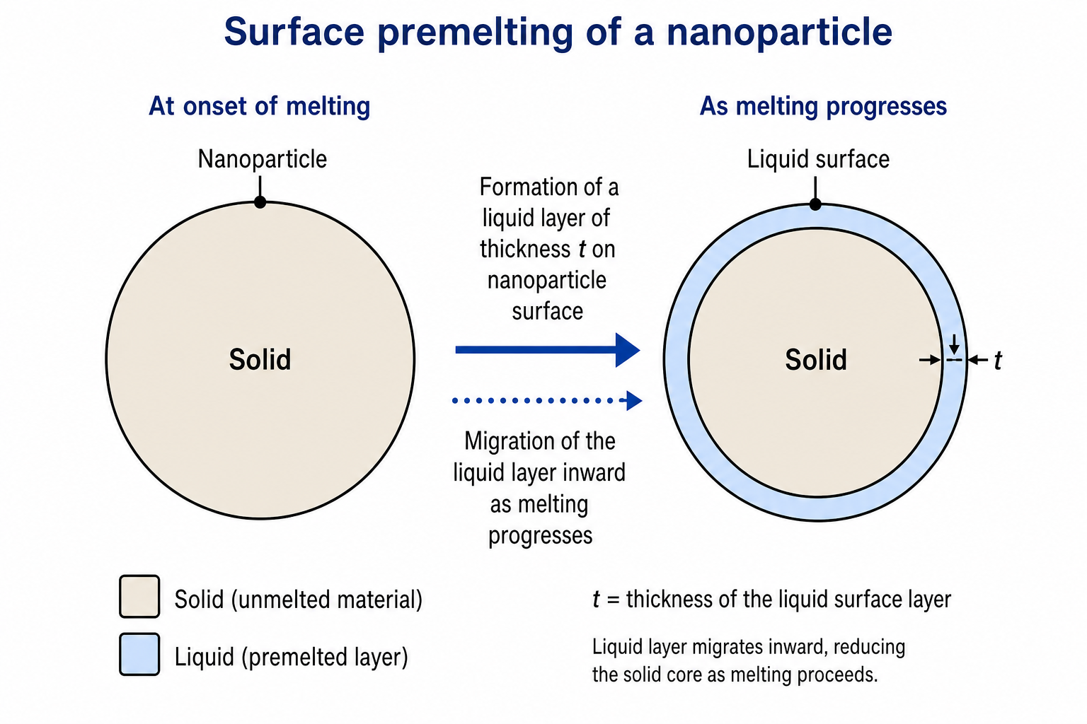
During this process three surface terms are simultaneously changed: a new liquid surface area AL is created (energy cost γL per unit area), a new liquid/solid interfacial area ASL is created (energy cost γSL per unit area), and the original solid surface area AS is destroyed (energy release γS per unit area). The total surface free energy change is therefore:
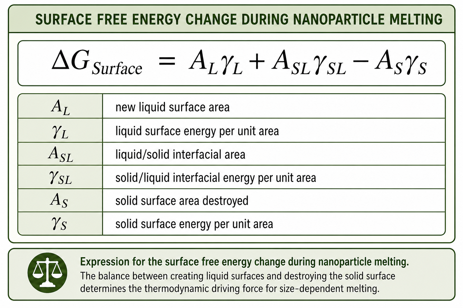
6 The Size-Dependent Melting Point Formula
At equilibrium the solid core of radius r has the same chemical potential as the surrounding liquid layer of thickness t. This condition is equivalent to requiring that the differential of the total free energy with respect to t vanishes: ∂ΔGTotal/∂t = 0. Imposing this gives the equilibrium condition:
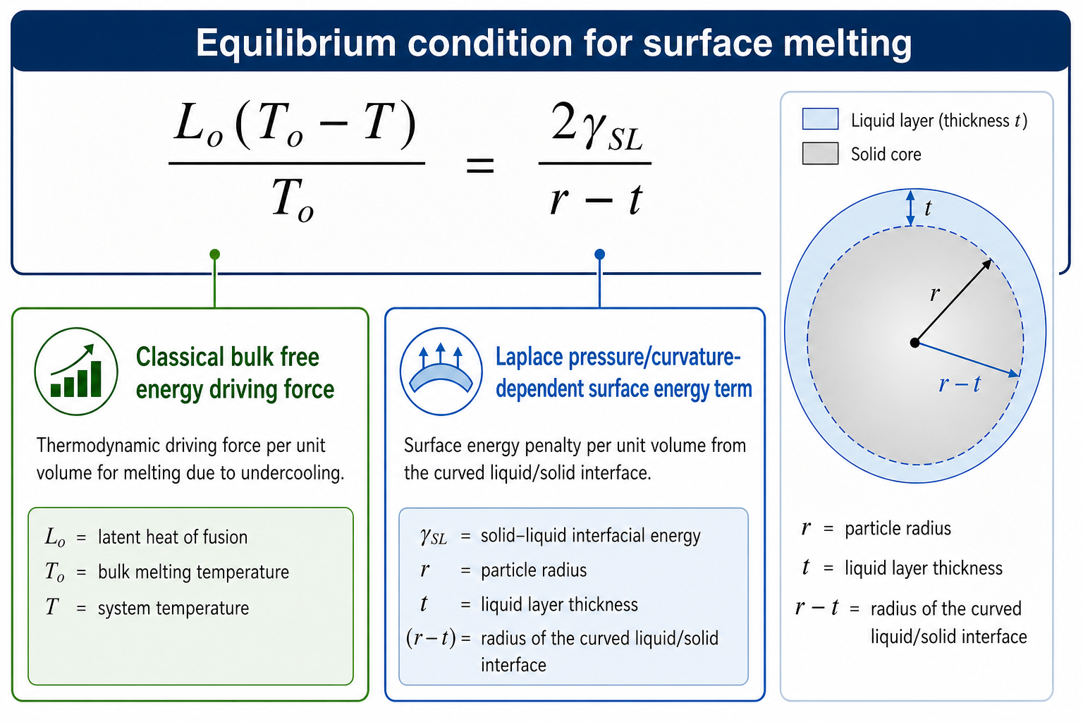
Taking the limit t → 0, which corresponds to the onset of the very first surface melting, the upper melting temperature for a spherical nanoparticle of radius r is obtained as:
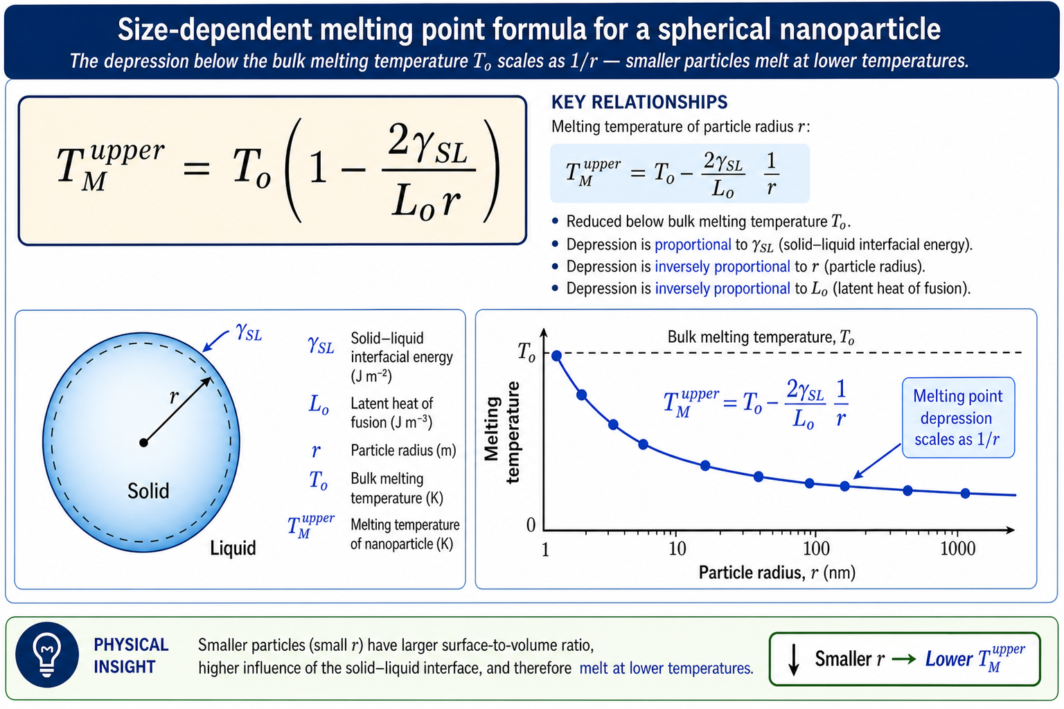
The melting point depression scales as 1/r. For a 5 nm radius gold nanoparticle this amounts to a reduction of roughly 100 K below the bulk melting point of 1337 K. The smaller the particle, the greater the depression — a direct consequence of the increasing importance of the surface free energy relative to the bulk latent heat.
7 Experimental Evidence: Melting Point vs Particle Size
The prediction that TM decreases monotonically with decreasing particle radius has been confirmed experimentally for a range of pure metals. The plots below show melting temperature as a function of particle radius for gold (Au), lead (Pb), copper (Cu), bismuth (Bi), and silicon (Si). In each case the calculated curve (from the formula above) and experimental data points agree well, converging to the bulk melting temperature (shown as a dashed horizontal line) as the radius exceeds ~30–50 nm. At radii below ~10 nm the depression is pronounced and strongly size-dependent.
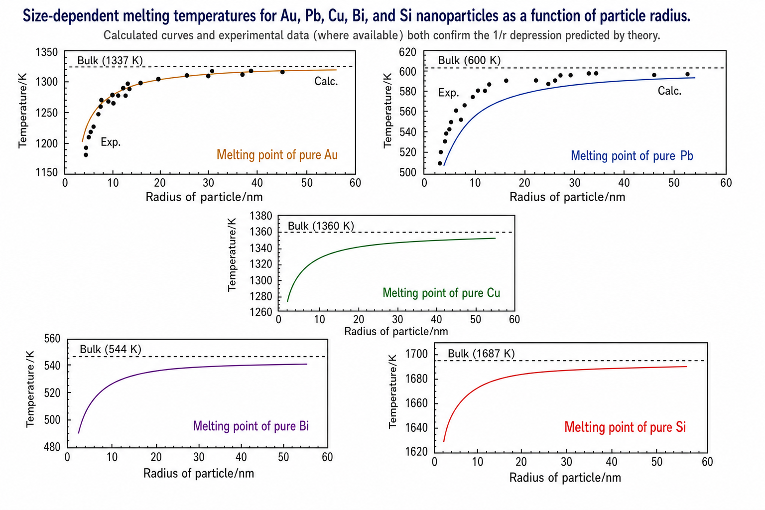
Bismuth and silicon are unusual among pure materials in that their liquid phases are denser than their solid phases — unlike most metals where the solid is denser. This means the Clausius–Clapeyron slope for their solid–liquid phase boundary is negative, and surface melting effects can in principle lead to either depression or, in constrained geometries, an elevation of the effective melting point. The data shown here capture the unconstrained free-particle melting behaviour.
- Ashby, M.F., Materials Selection in Mechanical Design, 4th ed., Butterworth-Heinemann, 2011.
- Vollath, D., Nanomaterials: An Introduction to Synthesis, Properties and Applications, Wiley-VCH, 2008.
- Pawlow, P., Z. Phys. Chem., 65, 1–35, 1909. (Original surface melting theory)
- Buffat, Ph. and Borel, J-P., Physical Review A, 13(6), 2287–2298, 1976. (Au nanoparticle melting experiments)
- Koch, C.C. (ed.), Nanostructured Materials: Processing, Properties and Applications, William Andrew, 2002.
- For deformation to occur, dislocations must penetrate grain boundaries; smaller grain size restricts pileup size and raises strength (Hall–Petch).
- At the amorphous extreme, crystal size shrinks to atomic dimensions, structure becomes fully disordered, and dislocation glide is replaced by shear-transformation-zone plasticity — giving maximum hardness and strength.
- Ashby charts show nanocrystalline metals, ceramic nanocomposites, metallic nanocomposites, and nanowires occupying strength fields far above conventional materials.
- Nano multilayers and amorphous metals approach the ideal strength (σy/E ≈ 10−1) — a fundamental ceiling that cannot be exceeded.
- In nanoscale solids the surface-to-volume ratio is large; melting must be treated as ΔGTotal = ΔGBulk + ΔGSurface.
- The melting point of a nanoparticle decreases as TMupper = To(1 − 2γSL/Lor) — smaller particles melt at lower temperatures.
- This 1/r depression is confirmed experimentally for Au, Pb, Cu, Bi, and Si nanoparticles and is a direct consequence of the increasing dominance of surface free energy over bulk latent heat at the nanoscale.
Melting in Nanocomposites & Thermal Transport in Nanomaterials
From the interfacial energy balance governing embedded nanoparticle melting to phonon confinement, group velocity, and size-dependent thermal conductivity in thin films and multilayers.
Contents
- Melting of Embedded Nanoparticles: The Matrix Effect
- Thermal Transport: Why Nanomaterials Are Different
- Group Velocity and Phonon Lifetime
- Dimension-Specific Phonon Effects and 2-D Nanomaterial Structures
- Thermal Conductivity of Single-Layered Nanofilms
- Multilayered Films: Interface Resistance, Doping, and Grain Boundaries
1 Melting of Embedded Nanoparticles: The Matrix Effect
In Lecture 18 we derived the size-dependent melting point for a free nanoparticle in contact with its own vapour. The result — TMupper = To(1 − 2γSL/Lor) — assumes the surrounding medium is effectively a gas, making γSL the only relevant interfacial energy. A natural follow-up question arises when we embed those same nanoparticles into a solid matrix to fabricate a nanocomposite: will they still melt below the bulk melting temperature of the parent material?
The answer is: not necessarily. When a nanoparticle sits inside a matrix its surface is in contact with a different solid, not with vapour. The relevant interfacial energy is now γSM, the solid-nanoparticle / matrix energy. The melting criterion is governed by a balance of three interfacial energies at the solid–liquid–matrix triple line, described by Young's equation: (γLM − γSM) / γSL = cos θ, where γLM is the liquid-nanoparticle / matrix energy, and θ is the contact angle of the liquid layer on the matrix surface.
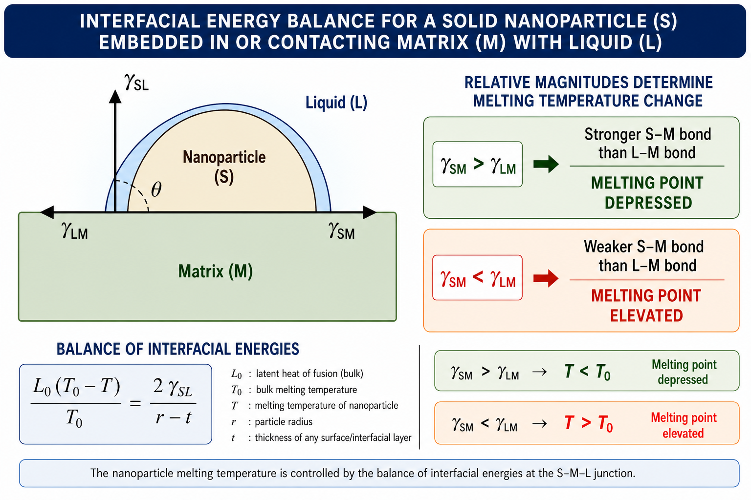
γSM > γLM : The solid/matrix interface is more costly than the liquid/matrix interface. Melting is promoted — the embedded nanoparticle melts below the bulk melting temperature.
γSM < γLM : The liquid/matrix interface is the costlier one. The solid surface is preferred and melting is suppressed — the embedded nanoparticle melts above the bulk melting temperature (superheating).
The melting temperature of an embedded nanoparticle can therefore be either increased or reduced with respect to the bulk material depending entirely on how γSL relates to the matrix through Young's equation. This has direct consequences for nanocomposite processing: the melting behaviour of dispersed particles cannot be read off a bulk phase diagram; it depends on the specific particle/matrix interface chemistry.
2 Thermal Transport: Why Nanomaterials Are Different
Thermal transport is one of the most application-critical properties of nanomaterials — and the requirements pull in opposite directions. In microprocessors, the goal is to remove heat as rapidly as possible (high thermal conductivity). In thermal barrier coatings and thermoelectrics, the goal is to impede heat flow (low thermal conductivity). In both cases, nanoscale engineering of the phonon population is the key tool.
In bulk materials, heat is carried by lattice vibration waves (phonons) in non-metals, and by free electrons in metals. Phonon scattering in non-metals is efficient — lattice vibrations can scatter easily — giving non-metals lower thermal conductivity than metals. When the system length scale is reduced to the nanoscale, two new regimes emerge simultaneously: quantum confinement of phonon modes, and enhanced classical scattering from the proliferating surfaces and interfaces. In a bulk homogeneous solid the phonon wavelengths are much smaller than the microstructural length scale. In a nanomaterial, the two length scales become comparable — completely changing the physics of heat transport.
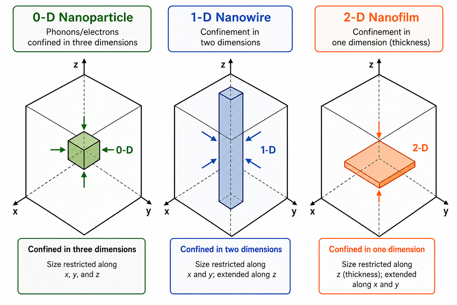
The presence of nearby surfaces in 0-D, 1-D, and 2-D nanostructures causes a change in the distribution of phonon frequencies as a function of wavelength, and introduces entirely new surface phonon modes that have no bulk analogue. Both effects modify how heat is carried.
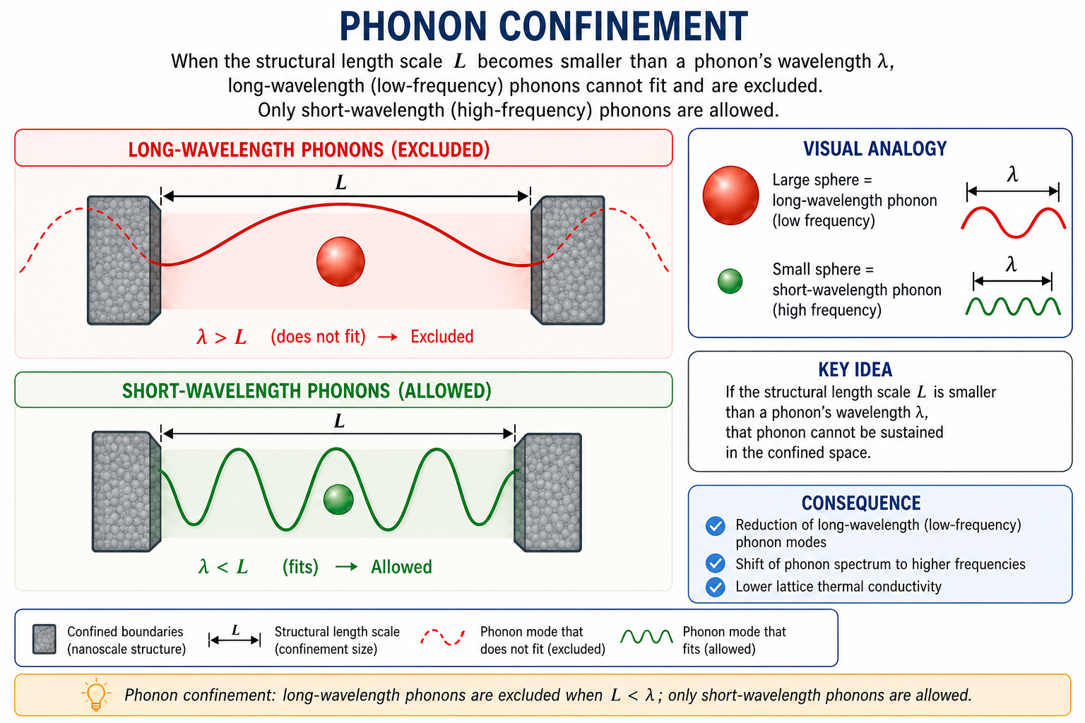
3 Group Velocity and Phonon Lifetime
Confinement and scattering modify two key quantities that together determine thermal conductivity: the group velocity and the phonon lifetime. The group velocity vg = dω/dk is the speed at which energy (the wave packet envelope) propagates — distinct from the phase velocity of the underlying oscillation. When a phonon wave packet propagates in a nanostructure, boundary conditions imposed by the finite geometry modify the dispersion relation ω(k) and therefore alter vg.
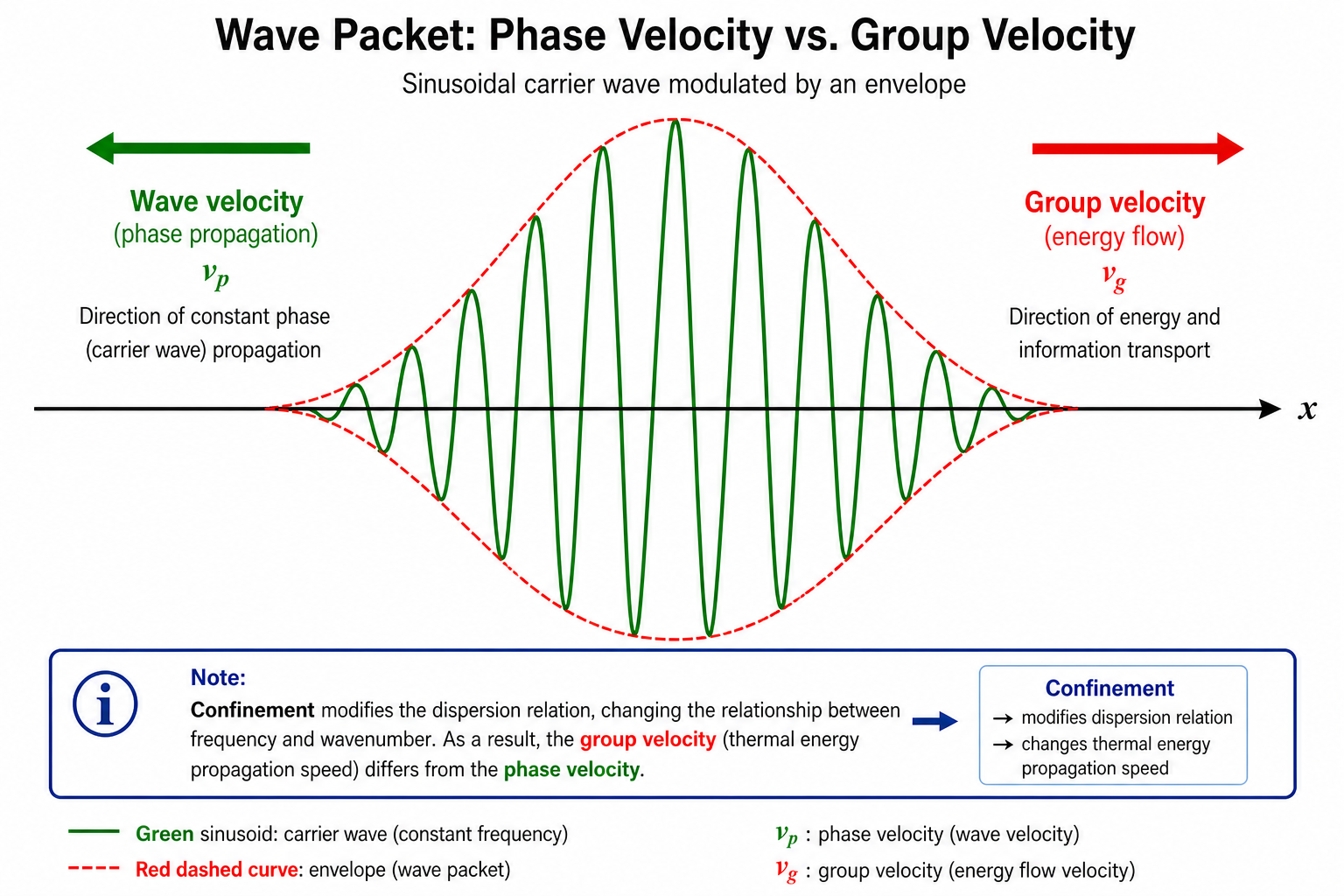
The phonon lifetime is also independently reduced in nanomaterials by three mechanisms: phonon–phonon Umklapp interactions, scattering from free surfaces (which proliferate as size decreases), and scattering from grain boundaries. Together these reduce the mean free path substantially below the bulk value.
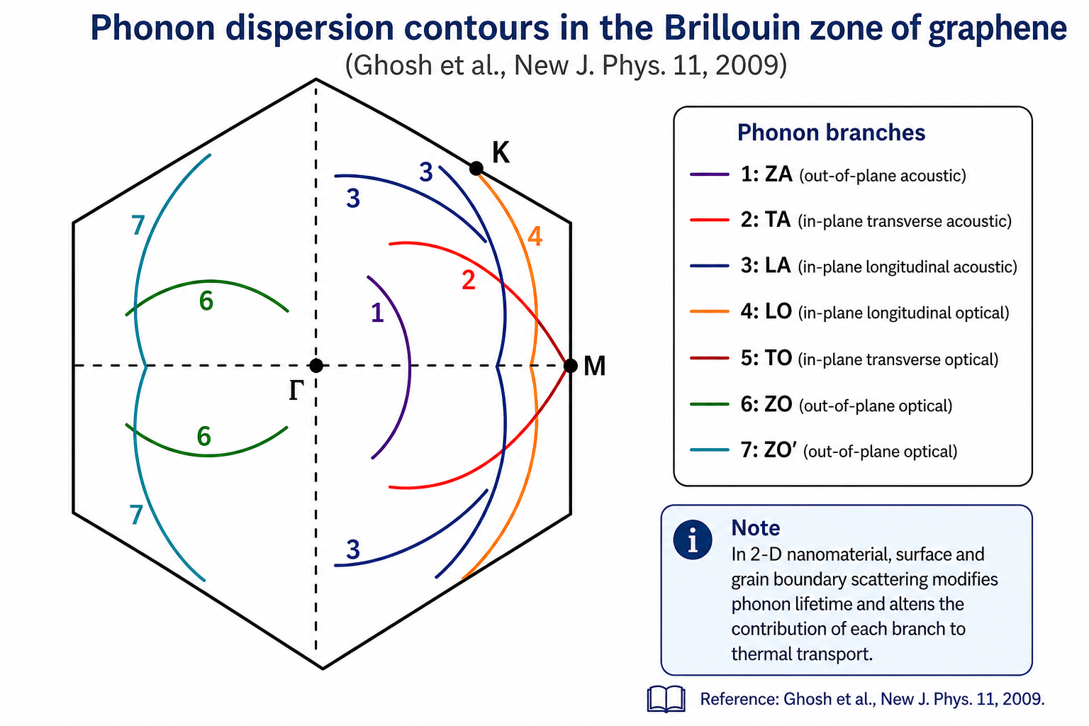
4 Dimension-Specific Phonon Effects and 2-D Nanomaterial Structures
In 0-D nanostructures a phonon bottleneck develops: quantised, sparse phonon modes limit how rapidly hot carriers can shed energy. In 1-D nanostructures (nanowires, nanotubes) phonons are guided along the axis as in a waveguide — efficient axial transport with surface scattering only in the radial direction. Carbon nanotubes have been predicted and measured to have axial thermal conductivities approaching 3000 W m−1 K−1, roughly seven times that of copper (~400 W m−1 K−1). In 2-D nanofilms, thermal conductivity is generally reduced below bulk values, with surface scattering the dominant mechanism.
2-D nanomaterials are of wide technological interest: components for handheld electronics, coatings for radiation shielding and wear resistance, thermal barriers, flat-panel displays, and photovoltaic devices. Structurally they fall into three categories: single-layered films with nanoscale thickness; multilayered stacks of several nanoscale layers; and thin films comprising a collection of nanostructured grains — the last of which may further be nanocrystalline or nanoporous (nanoporous films find use as low-dielectric-constant interlayer materials in microelectronics).
- 0-D (nanoparticles): Phonon bottleneck — quantised modes restrict heat dissipation.
- 1-D (nanowires, CNTs): Phonon waveguide — highly efficient axial transport; CNTs ~3000 W m−1 K−1.
- 2-D (nanofilms): Surface and interface scattering reduces conductivity below bulk; opposite temperature dependence to bulk.
5 Thermal Conductivity of Single-Layered Nanofilms
Measurements on single-layered nanoscale thin films almost universally show thermal conductivity below that of the corresponding bulk material — and the thinner the film, the lower the conductivity. This is a direct consequence of phonon scattering at the two free surfaces: as film thickness approaches and falls below the phonon mean free path, boundary scattering increasingly dominates over phonon–phonon scattering. Crucially, the temperature dependence is also reversed: bulk metals show conductivity that decreases with temperature, while nanofilms of the same material show conductivity that increases with temperature — because at low temperatures boundary scattering (independent of temperature) controls the mean free path rather than phonon–phonon interactions.
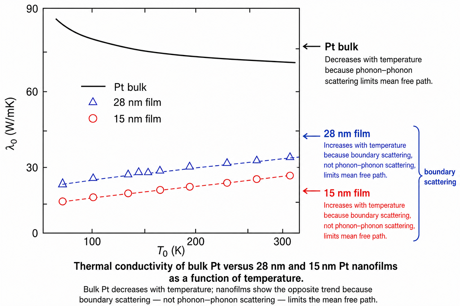
6 Multilayered Films: Interface Resistance, Doping, and Grain Boundaries
In multilayered thin films each interface is a disruption of the regular crystal lattice and introduces an additional thermal resistance. Even an interface between two crystals of the same material but different orientations presents a mismatch in the local phonon distribution, causing partial scattering and reflection of phonons that cross the boundary. When the two layers are dissimilar — different materials with different densities and sound velocities — the acoustic impedance mismatch produces partial phonon reflection at each interface, analogous to partial reflection of light at a glass surface. The more interfaces per unit thickness, the greater the cumulative scattering and the lower the effective thermal conductivity.
Alloying — adding dopant atoms — introduces local mass fluctuations and strain fields that scatter phonons just as grain boundaries do. The effect is particularly pronounced in polycrystalline silicon films, where grain boundary scattering already dominates. Adding dopants compounds the scattering, further suppressing conductivity. The overall strategy in nanostructured thermal management is to combine these mechanisms — layer interfaces, grain size, dopant concentration — to target different wavelength ranges of the phonon spectrum.
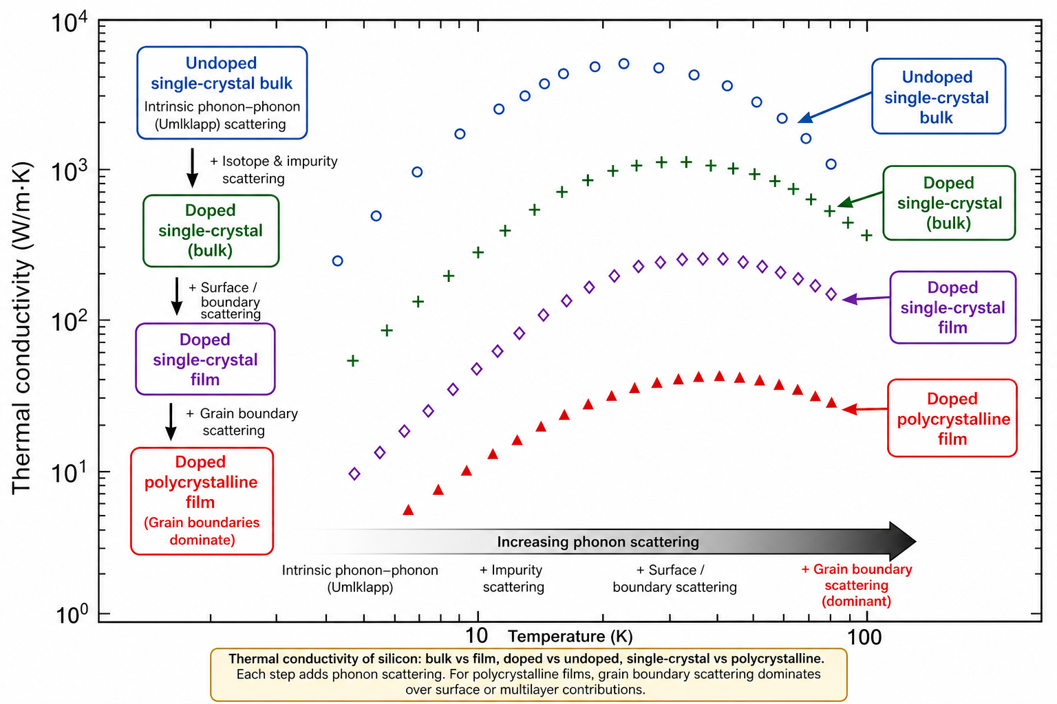
- Cahill, D.G. et al., Nanoscale thermal transport, J. Appl. Phys., 93(2), 793–818, 2003.
- Ghosh, S. et al., Heat conduction in graphene: experimental study and theoretical interpretation, New J. Phys., 11, 095012, 2009.
- Volz, S.G. (ed.), Thermal Nanosystems and Nanomaterials, Springer, 2009.
- Balandin, A.A., Thermal properties of graphene and nanostructured carbon materials, Nature Materials, 10, 569–581, 2011.
- Vollath, D., Nanomaterials: An Introduction to Synthesis, Properties and Applications, Wiley-VCH, 2008.
- Embedded nanoparticles melt below or above the bulk temperature depending on the sign of (γSM − γLM): if γSM > γLM, melting is depressed; if γSM < γLM, the particle is superheated above the bulk melting point.
- In nanomaterials the structural length scale approaches the phonon wavelength, activating quantum confinement and enhanced classical scattering simultaneously.
- Confinement modifies the phonon frequency distribution, introduces surface phonon modes, and alters the group velocity through changes in the dispersion relation.
- Phonon lifetime is reduced by phonon–phonon interactions, free surface scattering, and grain boundary scattering — all multiplied in a nanostructure.
- In 0-D structures a phonon bottleneck occurs; 1-D structures act as phonon waveguides (CNTs ~3000 W m−1 K−1); 2-D nanofilms show reduced conductivity with the opposite temperature dependence to bulk.
- In multilayered films, each interface adds thermal resistance; doping and grain boundaries add further scattering — for polycrystalline films, grain boundary scattering dominates.
Thermal & Electrical Properties of Nanomaterials
From nanoporous heat capacity anomalies and size-dependent thermal expansion to dimension-specific electron scattering, ballistic transport in CNTs, and quantum tunnelling as the conduction mechanism in 0-D networks.
Contents
- Completing the Thermal Picture: Alloying, Nanoporous Films, and Heat Capacity
- Heat Capacity and Thermal Expansion in Nanomaterials
- Electrical Properties: Bulk Background and Nanoscale Modifications
- Nanoscale Effects on Electrical Conductivity
- Dimension-Specific Electrical Conductivity: 3-D, 2-D, 1-D, 0-D
- Practical Contacts and Electron Tunnelling
1 Completing the Thermal Picture: Alloying, Nanoporous Films, and Heat Capacity
Lecture 19 closed with multilayered thin films and the way each interface adds thermal resistance. A complementary strategy for suppressing thermal conductivity is alloying — introducing solute atoms into the lattice creates local mass fluctuations and strain fields that scatter phonons across a broad wavelength range. The effect is particularly striking in polycrystalline silicon films, where grain boundary scattering already dominates: adding dopant atoms (doping) compounds the scattering and drives conductivity down further still. The combined picture is a hierarchy of phonon-scattering mechanisms — surface, multilayer interface, grain boundary, and point-defect/dopant — each targeting a different part of the phonon spectrum, and the overall strategy of nanoscale thermal engineering is to deploy these in combination.
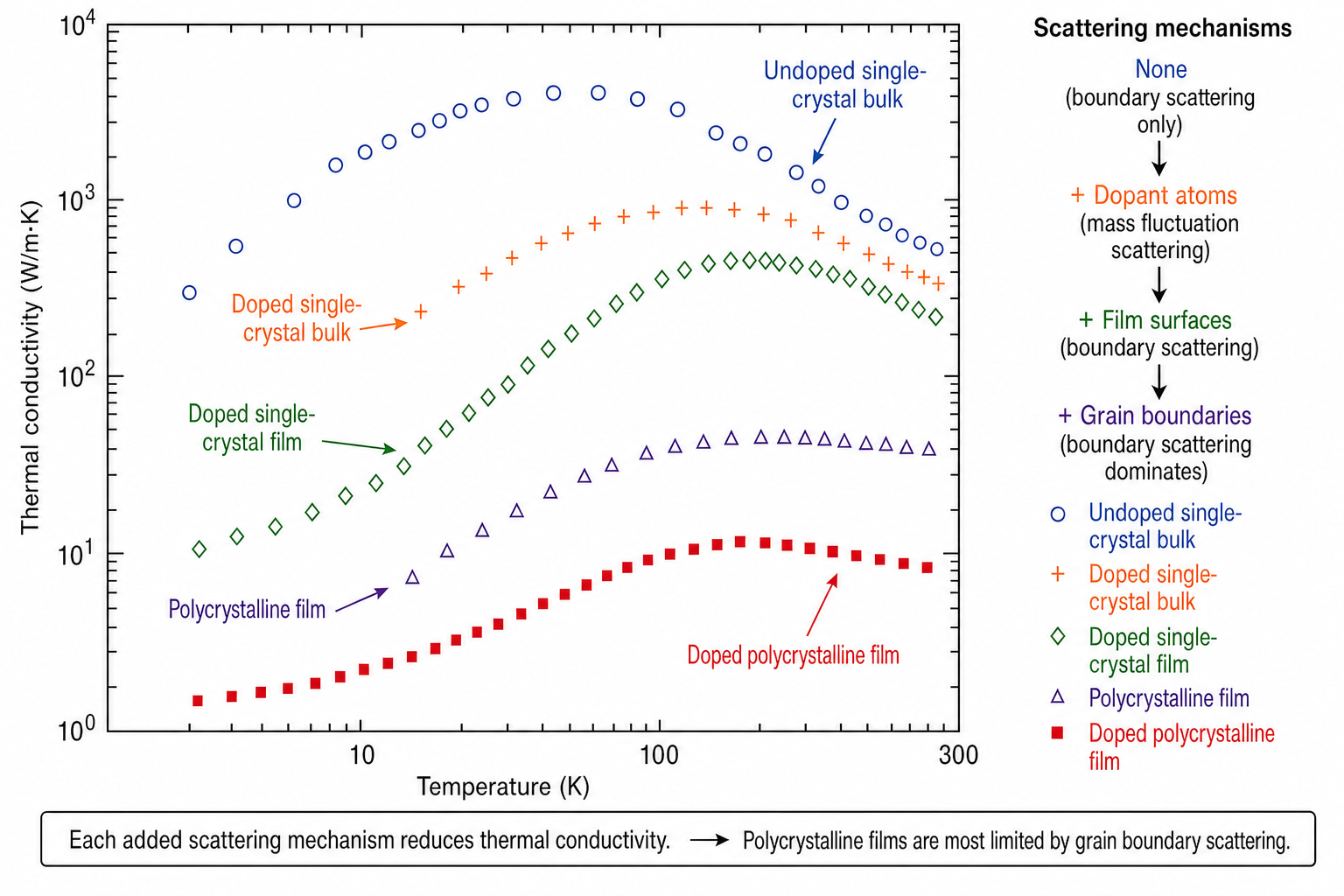
A distinct class of 2-D nanostructure is the nanoporous film. Here the thermal and dielectric properties are controlled by the number and size of the pores rather than by grain size or layering. Nanoporous materials have low permittivity and low thermal conductivity — both attractive for microelectronic interlayer applications — but in active circuit components the reduced heat-removal capability raises operating temperatures and accelerates failure. A key physical reason for the unusual phonon behaviour is that the pore size and the relevant phonon wavelengths become comparable: phonons passing through a nanoporous medium no longer experience a spatially homogeneous continuum field, and the standard bulk scattering formulae break down.
To suppress thermal conductivity across the full phonon spectrum, engineers combine: surface scattering (targets long-wavelength phonons), multilayer interfaces (targets mid-wavelength), grain boundaries (broad-band), and dopant/alloying point defects (targets short-wavelength). Nanoporous films add a further mechanism — geometric scattering — effective when pore diameter approaches phonon wavelength.
2 Heat Capacity and Thermal Expansion in Nanomaterials
Nanocrystalline iron was found experimentally to exhibit an enhanced heat capacity relative to coarse-grained polycrystalline iron. The accepted explanation is an entropy contribution to the heat capacity arising from the large fraction of grain boundary atoms — these atoms sit in positions with higher configurational and vibrational disorder than bulk-interior atoms, contributing additional degrees of freedom to the thermal energy budget.
A more nuanced picture emerges from nano ZnO flakes compared with coarse ZnO. In the low-temperature range 83–103 K the nano flakes show a lower heat capacity than coarse grains — an anomaly that remains difficult to explain fully. Above 103 K the relationship inverts: nano flakes show higher heat capacity than coarse grains, attributed to the configuration and vibration entropy of grain boundaries, consistent with the iron result. The crossover temperature reflects the interplay between quantum size effects (which suppress low-temperature heat capacity) and grain-boundary entropy contributions (which enhance it).
83–103 K: nano ZnO flakes Cp < coarse grain Cp — origin not fully explained; likely related to quantum confinement suppressing low-energy phonon modes.
Above 103 K: nano ZnO flakes Cp > coarse grain Cp — grain boundary configuration and vibration entropy dominates.
The coefficient of thermal expansion (CTE) is also size-dependent. Silver nanoparticles of 3.2 nm average diameter embedded in glass showed an enhanced expansion parameter with temperature compared with bulk silver — driven by the high surface-to-volume ratio and the mechanical constraints imposed by bonds across the particle–glass interface. Silver particles of 5.1 nm showed no significant deviation from bulk behaviour, indicating that the CTE enhancement is confined to the smallest size regime where interfacial bonds constitute a substantial fraction of all bonds. For carbon nanotubes, the CTE is exceptionally low: in-plane bond stretching and bond bending effects partially cancel each other, suppressing net thermal expansion.
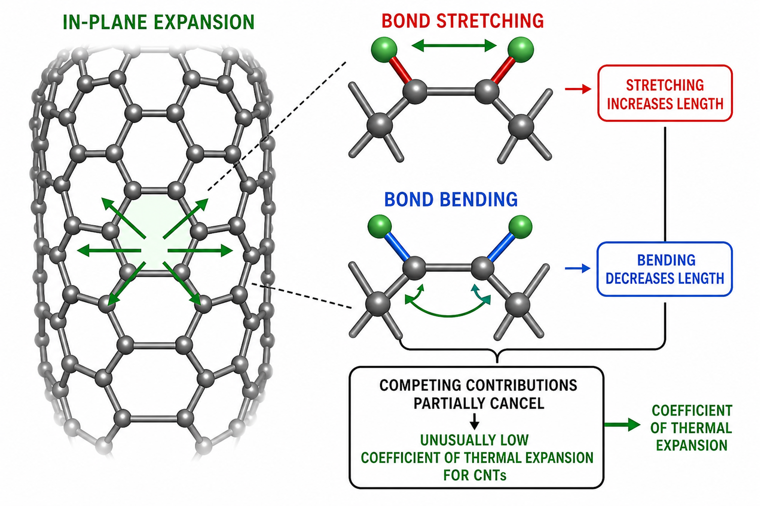
3 Electrical Properties: Bulk Background and Nanoscale Modifications
In a bulk metal, conduction electrons are delocalized — free to move through all three spatial dimensions. As they travel, they are scattered by several mechanisms: phonons (lattice vibrations), impurities (point defects, dopants), and interfaces (grain boundaries, surfaces). These scattering events interrupt the electron's trajectory and collectively produce the electrical resistance of the material, resembling a random-walk process.
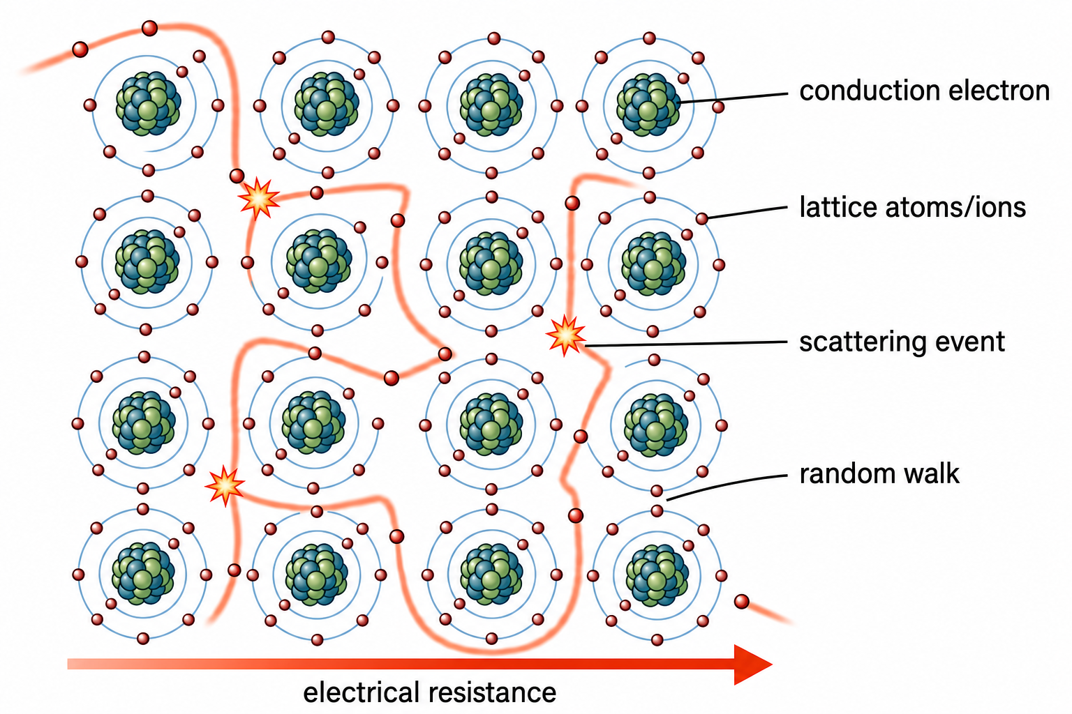
Three primary scattering channels can be distinguished. In electron–phonon scattering, an electron collides with a lattice site, creates a phonon of wavevector k, and the two electrons involved exchange momentum accordingly (k1 → k1−k and k2 → k2+k). In electron–interface scattering, hot electrons crossing a grain boundary or moving past a nanoparticle or atomic defect are deflected and lose energy. In electron–impurity scattering, a substitutional solute atom (or vacancy) disrupts the local periodicity, creating a polarization cloud or strain field that deflects passing electrons.
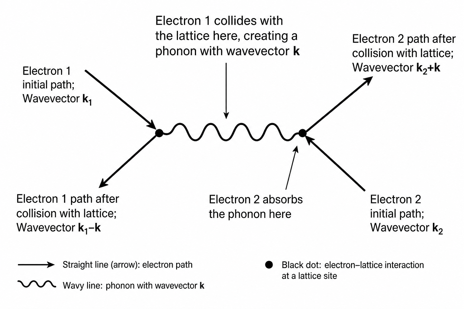
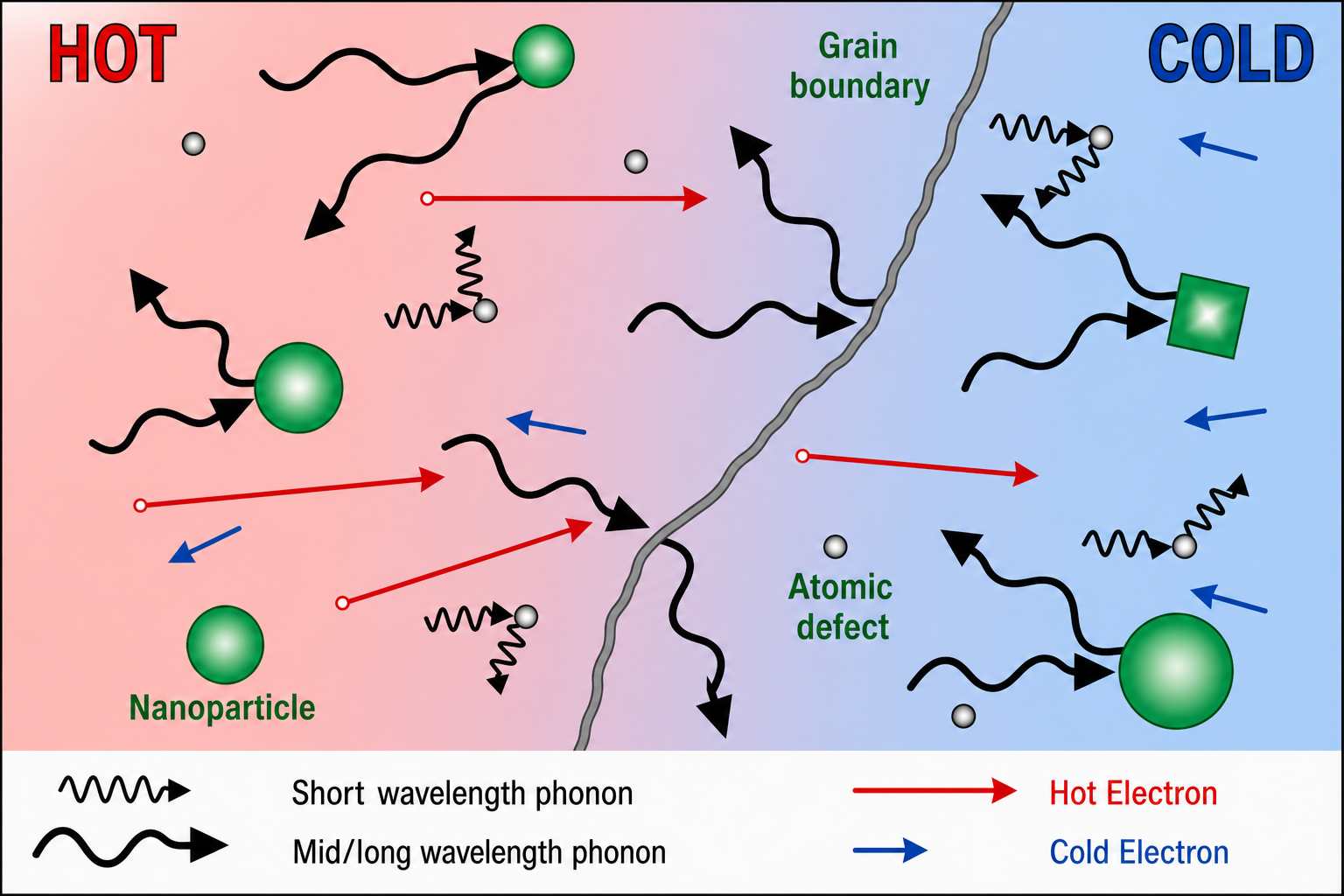
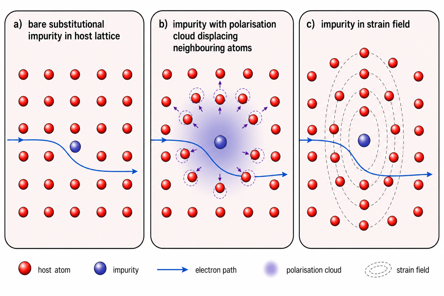
4 Nanoscale Effects on Electrical Conductivity
When the structural dimensions of a material fall to the nanoscale, two distinct mechanisms modify electrical conductivity. The first is the quantum effect: electron confinement in reduced dimensions forces the available energy states to become discrete rather than continuous. This quantisation can cause materials that are metallic conductors in their bulk form to behave as semiconductors or even insulators — a striking reversal of expected behaviour driven purely by size. The second is the classical effect: the mean free path for inelastic electron scattering becomes comparable with the physical dimensions of the system, changing the statistics of scattering events and reducing their overall rate. Both effects are negligible in a bulk 3-D material with large grains, but in a nanostructure the large grain boundary area-to-volume ratio means scattering at grain boundaries and interfaces dominates over bulk phonon scattering, and neither quantum nor classical corrections can be ignored.
Quantum effect: electron confinement produces discrete energy levels. Conducting materials can become semiconductors or insulators. Strongest in 0-D and 1-D nanostructures.
Classical effect: mean free path ≈ system size → reduction in scattering event rate. Grain boundary area-to-volume ratio is large → grain boundary scattering dominates in 3-D nanocrystalline materials.
5 Dimension-Specific Electrical Conductivity: 3-D, 2-D, 1-D, 0-D
Case 3-D (bulk nanocrystalline): Nanosize grains give a high grain boundary area-to-volume ratio, increasing electron scattering at grain boundaries. The result is a systematic reduction in electrical conductivity compared with a coarse-grained polycrystal of the same composition.
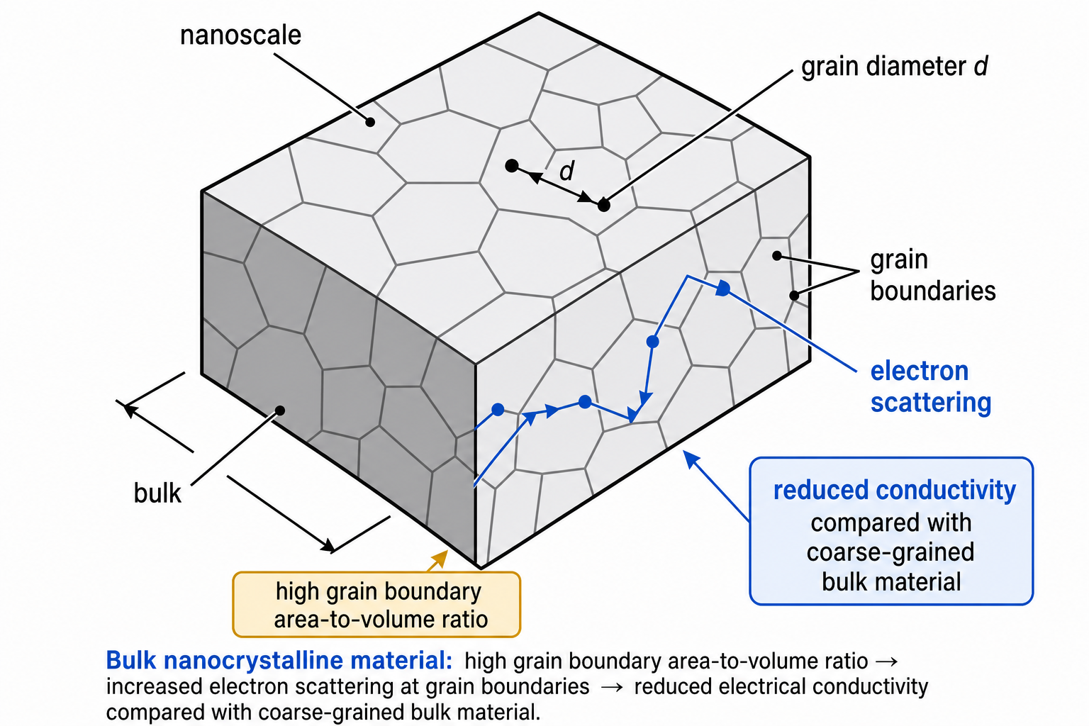
Case 2-D (nanocrystalline thin films, t ≤ 100 nm): Quantum confinement acts along the thickness direction, leaving carrier motion uninterrupted in the plane of the sheet. As a consequence, phonon and impurity scattering is restricted to the in-plane directions. Grain boundaries within the film provide an additional in-plane scattering source. The combined result is: the smaller the in-plane grain size, the lower the electrical conductivity of 2-D nanocrystalline films.
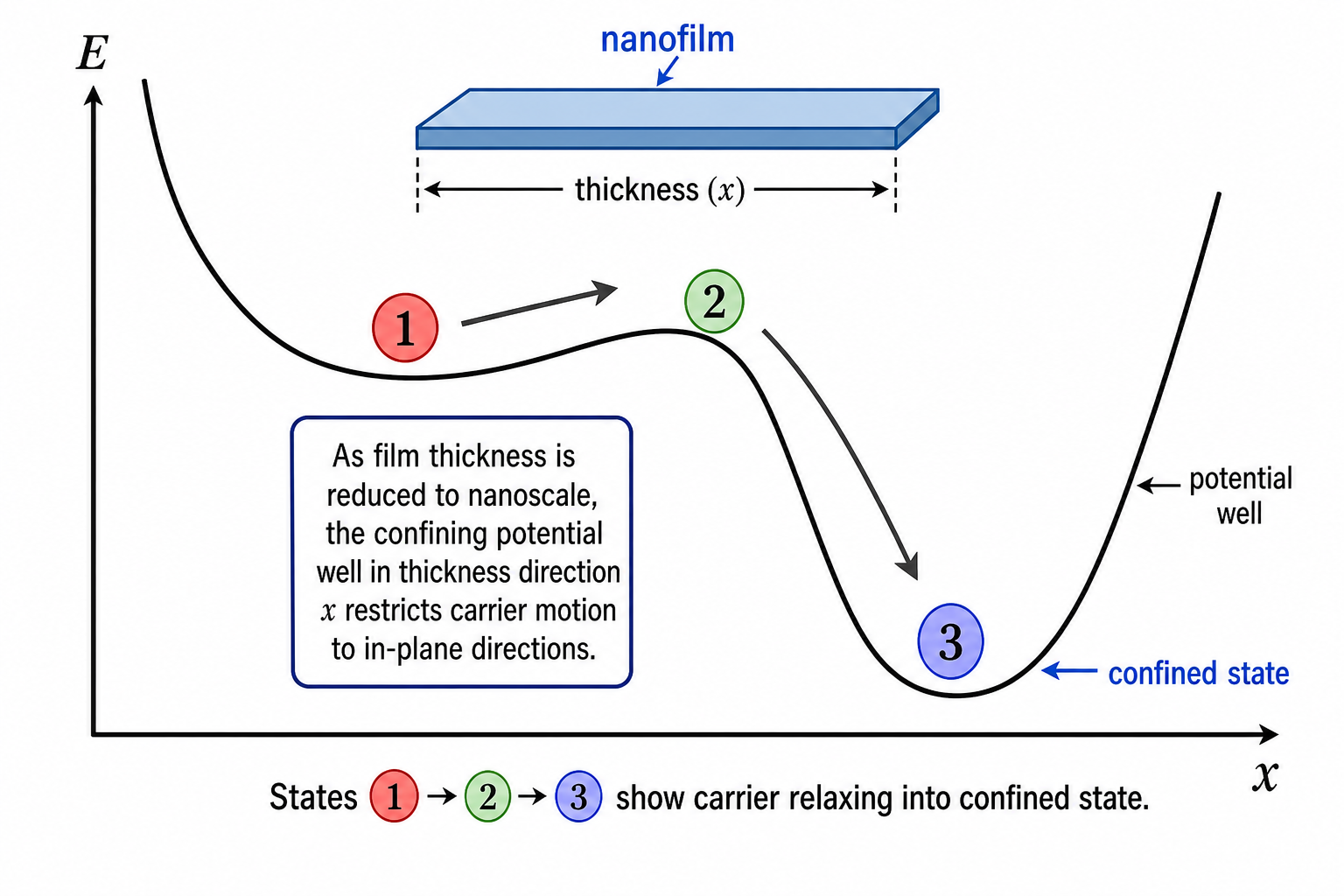
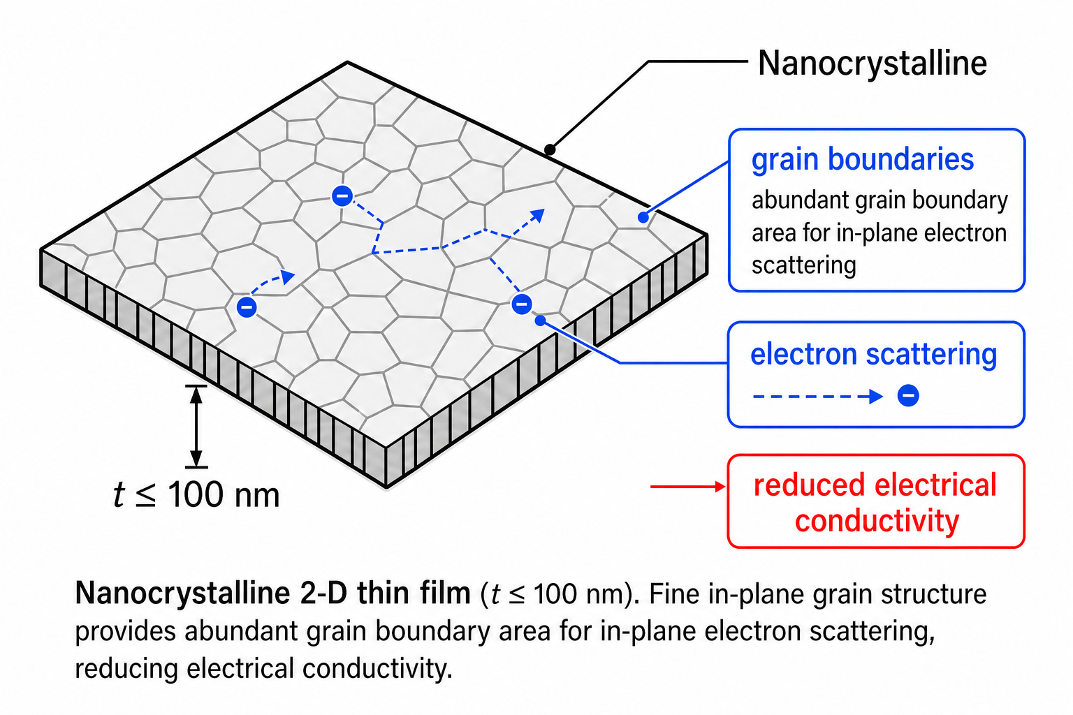
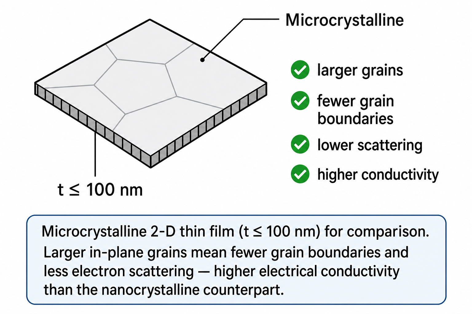
Case 1-D (nanowires, nanorods, nanotubes, d ≤ 100 nm): Quantum confinement acts in two dimensions — the two radial directions — leaving free carrier motion only along the long axis. Because of this confinement geometry, the nanoscale radial dimensions act as electron reflectors, preventing electrons from exiting through the surfaces. Although boundary scattering is in principle more pronounced due to the high surface-to-volume ratio of 1-D structures, scattering by impurities and phonons is itself restricted to the axial direction. The net result is that electron transport along the tube axis occurs without significant kinetic energy loss — this is ballistic transport. Carbon nanotubes (CNTs) are the paradigm case: their current-carrying capacity reaches ~109 A cm−2, roughly 1000 times greater than copper (~106 A cm−2).
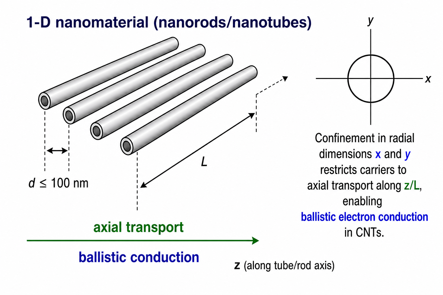
Case 0-D (nanoparticles, d ≤ 100 nm): Electron motion is totally confined in all three spatial dimensions. All energy states become discrete — no electron delocalization occurs. Under these conditions a metallic system can develop an energy band gap (not present in bulk form), causing it to behave as an insulator. This metal-to-insulator transition driven purely by size reduction is one of the most striking manifestations of quantum confinement in 0-D nanomaterials.
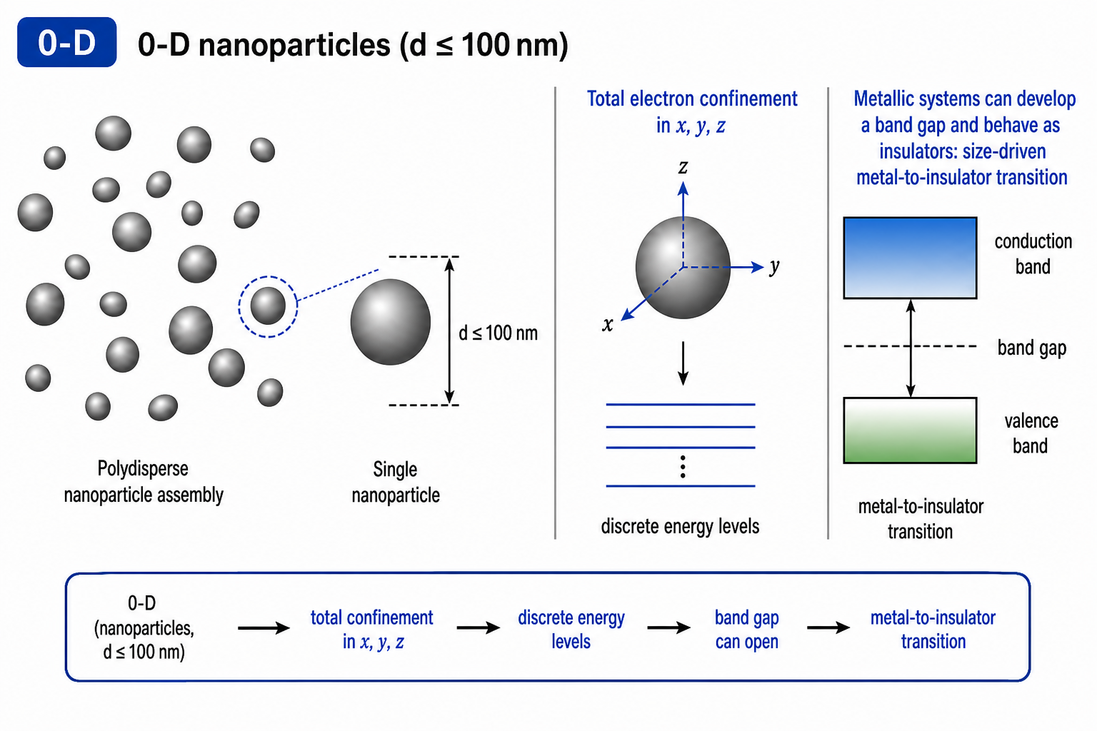
- 3-D nanocrystalline: High grain boundary area-to-volume ratio → increased grain boundary scattering → reduced σ.
- 2-D nanofilm: Confinement in thickness; in-plane scattering by phonons, impurities, and grain boundaries dominates → smaller grain size = lower σ.
- 1-D nanowire/CNT: Confinement in two radial dimensions → ballistic axial transport; CNTs carry ~109 A cm−2 vs 106 A cm−2 for Cu.
- 0-D nanoparticle: Full 3-D confinement → discrete energy states → metallic systems can open a band gap and become insulators.
6 Practical Contacts and Electron Tunnelling
From a device perspective, nanomaterials must be electrically coupled to external circuits through electrodes. For 2-D and 3-D nanomaterials, forming ohmic contacts is straightforward. For 0-D and 1-D nanomaterials, contact resistances are high because the structural features of the nanostructure — discretised energy states, nanometre dimensions — make conventional ohmic coupling difficult.
In such systems the dominant conduction mechanism is electron tunnelling — a quantum mechanical effect in which an electron penetrates a potential barrier higher than its classical kinetic energy would permit. Rather than being reflected at the barrier, the electron's wavefunction decays exponentially through it, with a non-zero probability of appearing on the other side. This is illustrated by the metal–insulator–metal (MIM) junction geometry, where two metallic conductors are separated by an insulating layer a few nanometres thick and a measurable current flows through the insulator by tunnelling even at low applied voltages.
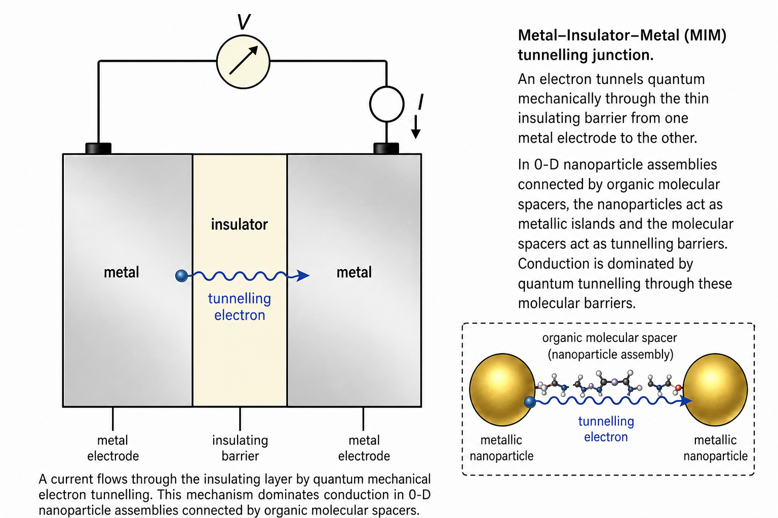
A practical example of tunnelling conduction is gold nanoparticle networks. When Au nanoparticles (conductors) are electrically coupled to one another through short organic molecules (insulators), the measured conductance is significantly higher than expected for a classical insulating barrier — the enhancement is attributed entirely to electron tunnelling through the organic spacer. By contrast, Au nanoparticles that are not coupled by organic molecules show much lower inter-particle conductance, confirming that the molecular bridge is the tunnelling pathway.
- Vollath, D., Nanomaterials: An Introduction to Synthesis, Properties and Applications, Wiley-VCH, 2008.
- Cahill, D.G. et al., Nanoscale thermal transport, J. Appl. Phys., 93(2), 793–818, 2003.
- Dresselhaus, M.S. et al., Perspectives on carbon nanotubes and graphene Raman spectroscopy, Nano Letters, 10(3), 751–758, 2010.
- Thellung, A., Phonons and the thermal properties of solids, in Thermal Nanosystems and Nanomaterials, ed. Volz, S.G., Springer, 2009.
- Schmid, G. (ed.), Nanoparticles: From Theory to Application, Wiley-VCH, 2004.
- Alloying introduces phonon-scattering point defects; combined with grain boundaries and interfaces it enables full-spectrum phonon management. Nanoporous films use geometric scattering when pore size ≈ phonon wavelength.
- Nanocrystalline materials show enhanced heat capacity due to grain-boundary entropy; CTE is enhanced in the smallest Ag nanoparticles (3.2 nm) due to interfacial bonding, but unaffected at 5.1 nm. CNTs have near-zero CTE due to competing bond-stretching and bond-bending effects.
- Electron scattering in bulk metals occurs via phonons, impurities, and interfaces; in nanocrystalline materials grain boundary scattering dominates over all others.
- Two nanoscale effects on conductivity: quantum confinement (discrete energy states, potential band-gap opening) and classical mean-free-path effects (reduced scattering rate when MFP ≈ system size).
- 3-D nanocrystalline → reduced σ. 2-D nanofilm → in-plane scattering, smaller grains = lower σ. 1-D CNT → ballistic transport, ~109 A cm−2. 0-D nanoparticle → discrete states, metallic systems can become insulators.
- For 0-D and 1-D nanostructures the dominant conduction mechanism across contacts is electron tunnelling through the potential barrier separating particle from electrode or particle from particle.
Magnetic Properties of Nanomaterials
From the four energy terms governing nanoscale magnetisation and the origin of ferromagnetism, through hysteresis loops, domain wall physics, and anisotropy energy, to the critical grain size, superparamagnetism, and how size reduction reshapes the coercive field.
Contents
- Electron Tunnelling Revisited: STM and Wavelength Modification
- Magnetic Energy Terms for Nanoscale Ferromagnets
- Why Ferromagnetic Materials?
- Role of Temperature: The Curie Point
- The M–H Hysteresis Loop
- Physical Significance of Each Energy Term
- Domain Walls vs Grain Boundaries
- Nanoscale Magnetic Behaviour: Critical Grain Size and Superparamagnetism
- Effect of Grain Size on Coercive Field
1 Electron Tunnelling Revisited: STM and Wavelength Modification
Lecture 20 closed with electron tunnelling as the dominant conduction mechanism in 0-D nanoparticle networks. This lecture opens by deepening that picture. In the scanning tunnelling microscope (STM), a sharp conducting tip is brought within a nanometre of a conducting surface and a bias voltage is applied. Even though the gap between tip and surface is a classically forbidden region, electrons tunnel across it, producing a measurable tunnel current that is exquisitely sensitive to tip–surface distance. This is the quantum mechanical effect at work in a real instrument.
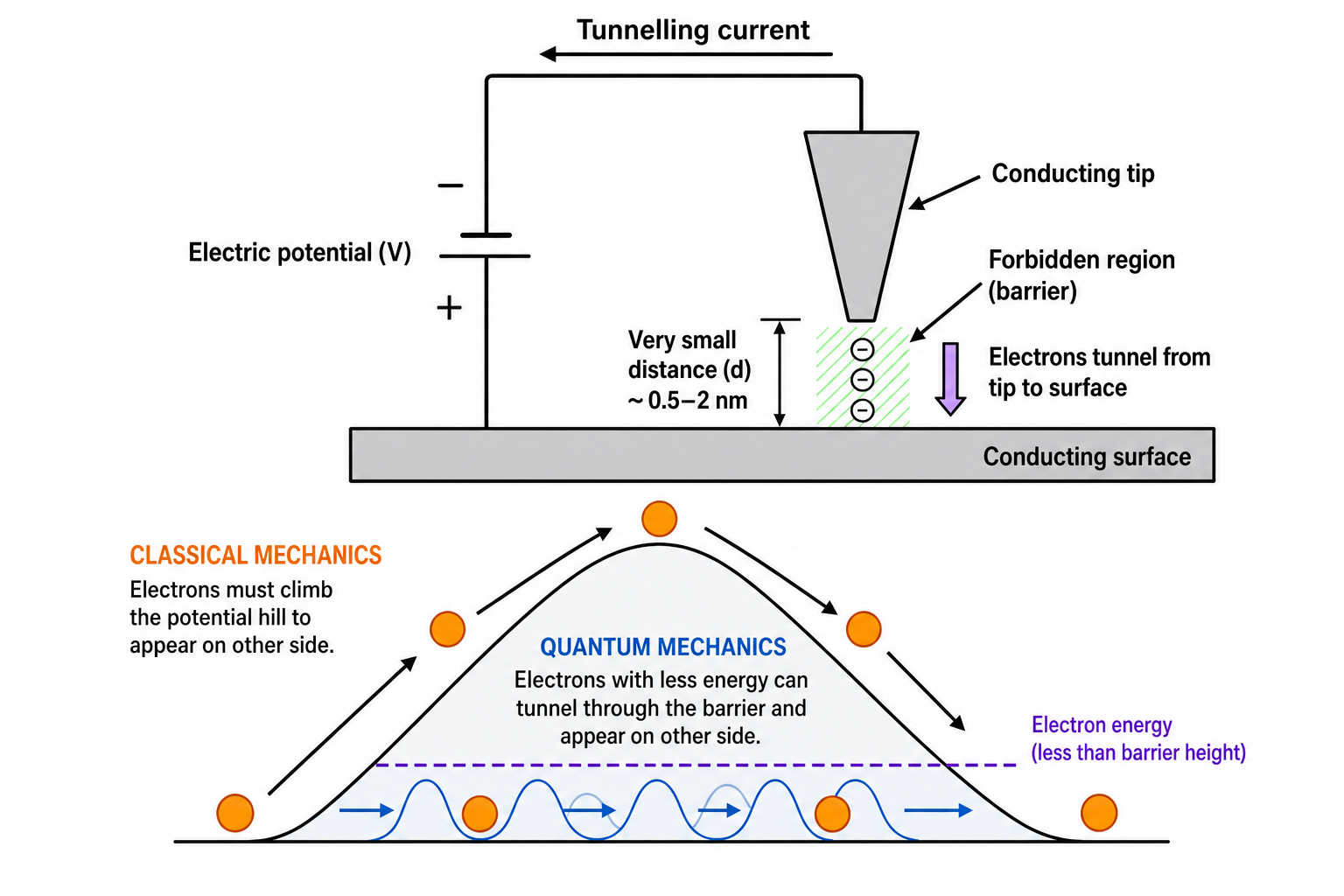
A complementary effect is the modification of electron wavelength at an interface. When an electron crosses into a region of different potential (such as the insulating interlayer of an MIM junction), its de Broglie wavelength changes abruptly. The upper panel of the wavelength diagram shows the wave truncating at a thick barrier — the electron cannot penetrate. The lower panel shows that for a thinner barrier the wavelength is modified but the electron emerges on the other side, its wavefunction attenuated but nonzero. This is quantum mechanical tunnelling in its wave-picture form.
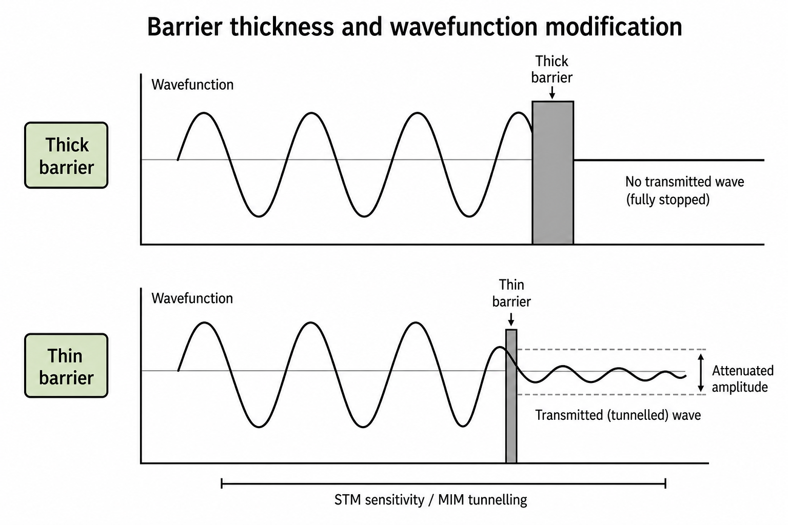
2 Magnetic Energy Terms for Nanoscale Ferromagnets
For any ferromagnetic material at the nanoscale, the total magnetisation energy has four contributions:
Etotal = Eexc + Eani + Edem + Eapp
Eexc — exchange energy: the quantum mechanical interaction that drives neighbouring spins to align parallel, giving rise to spontaneous magnetisation.
Eani — anisotropy energy: the tendency of spins to align along specific crystallographic "easy axes" rather than arbitrary directions.
Edem — demagnetisation energy: the dipole energy of the magnetised body, which drives the formation of magnetic domains to minimise the external stray field.
Eapp — applied field energy: the interaction between the magnetisation vector and an externally applied field H, given by Etotal = M·H.
For macroscopic magnetic materials a fifth term — magnetostrictive energy (magnetic ↔ mechanical coupling) — must also be included. This term is less significant at the nanoscale because domain structures are suppressed.
The magnetisation energy is also expressible as Etotal = M·H, where M is the magnetisation vector and H the applied field. Magnetic fields arise from two sources: (a) moving electric charge in electromagnets (right-hand rule), and (b) electron spin in atoms of intrinsically magnetic materials (left-hand rule for force on a current).
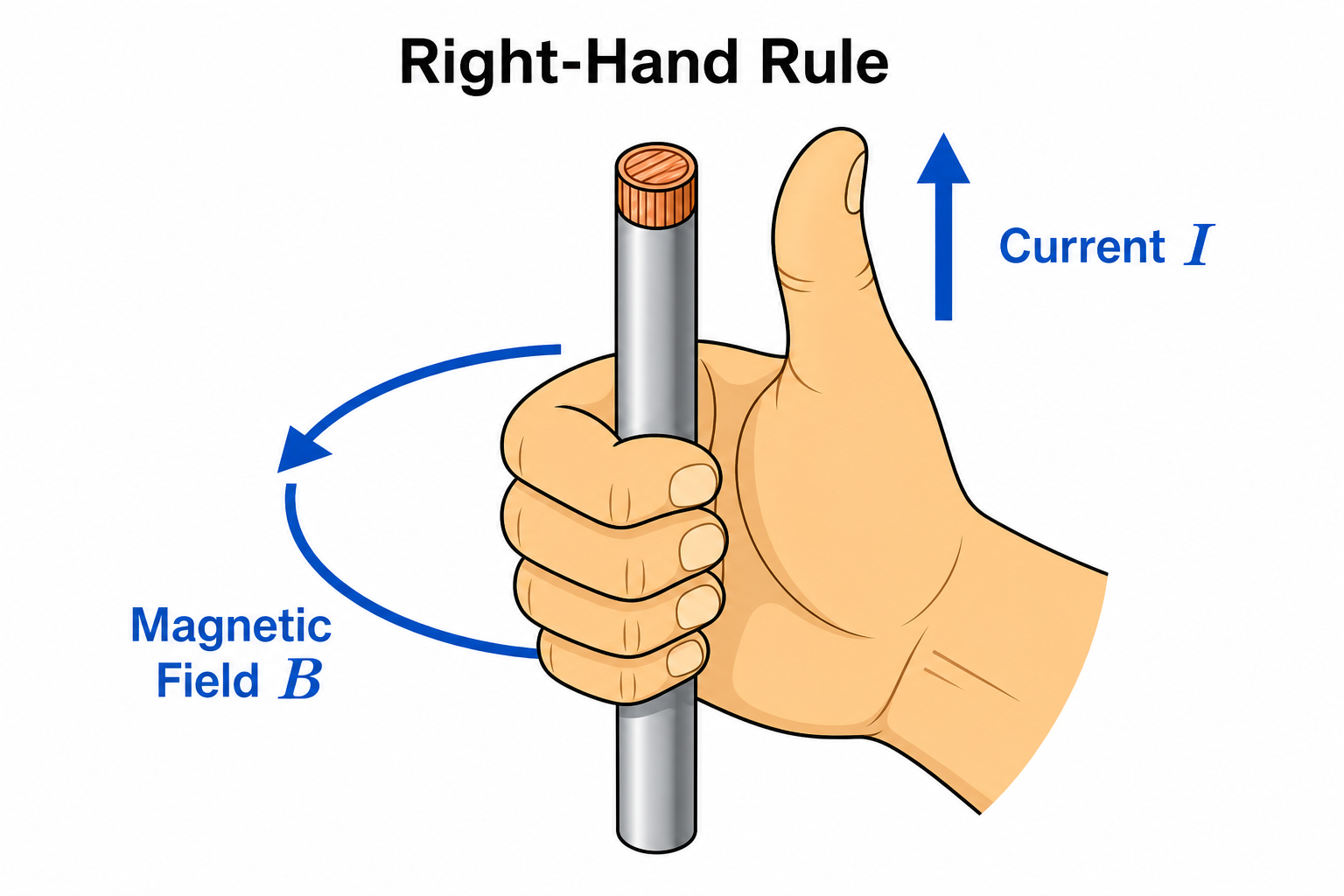
3 Why Ferromagnetic Materials?
Nearly all materials respond to a magnetic field by becoming magnetised, but most are paramagnetic — Al and Pt are examples — with a response so faint that it has no practical utility. In paramagnetic materials, atomic magnetic moments interact so weakly that ordinary thermal motion is sufficient to randomise their orientations, producing no net moment in the absence of an applied field.
A small subset of materials, however, contain atoms with large magnetic dipole moments and the ability to spontaneously magnetise — that is, to align their dipoles in parallel without any applied field. These are the ferromagnetics: Ni, Fe, and Co are the archetypal examples. The driving force is the exchange interaction: when neighbouring atomic moments align, the system lowers its energy by Eexc. If this exchange energy exceeds the randomising thermal energy at a given temperature, spontaneous alignment is maintained.
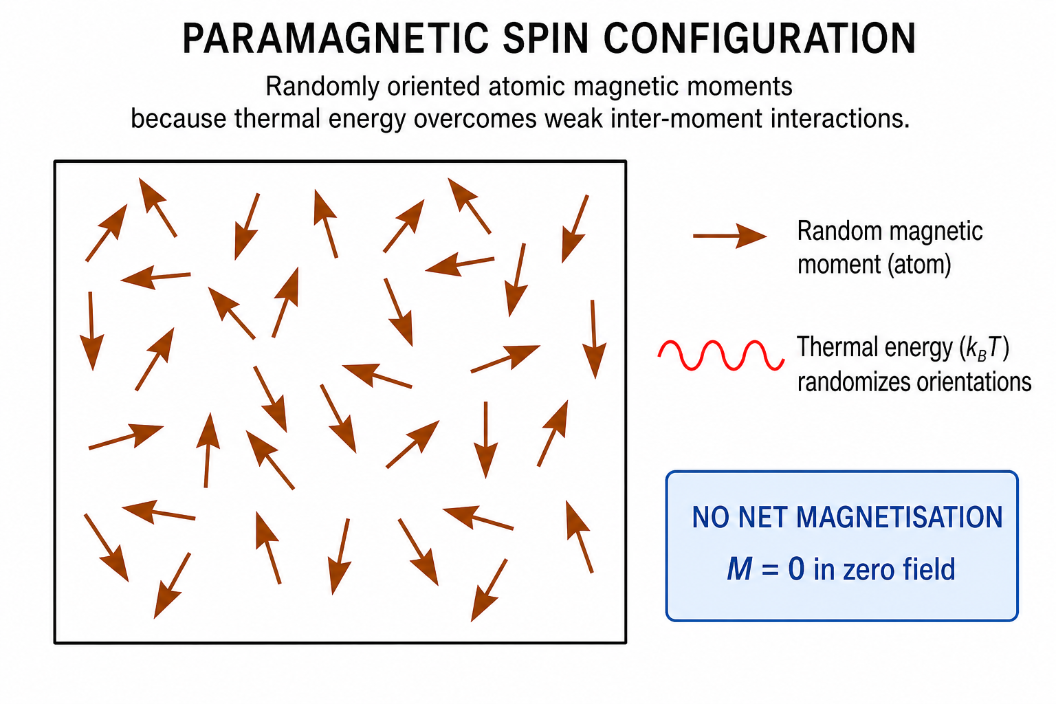
If neighbouring moments align antiparallel (head to tail), the net moment is zero — these materials are antiferromagnetic. If all spins align parallel, the net moment is maximised — these are ferromagnetic.
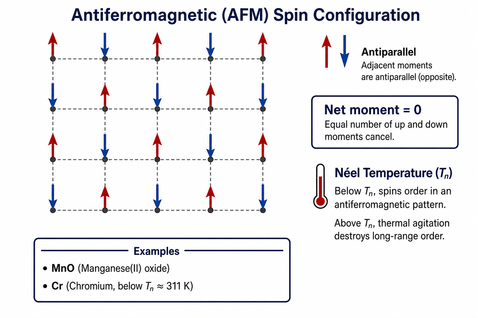
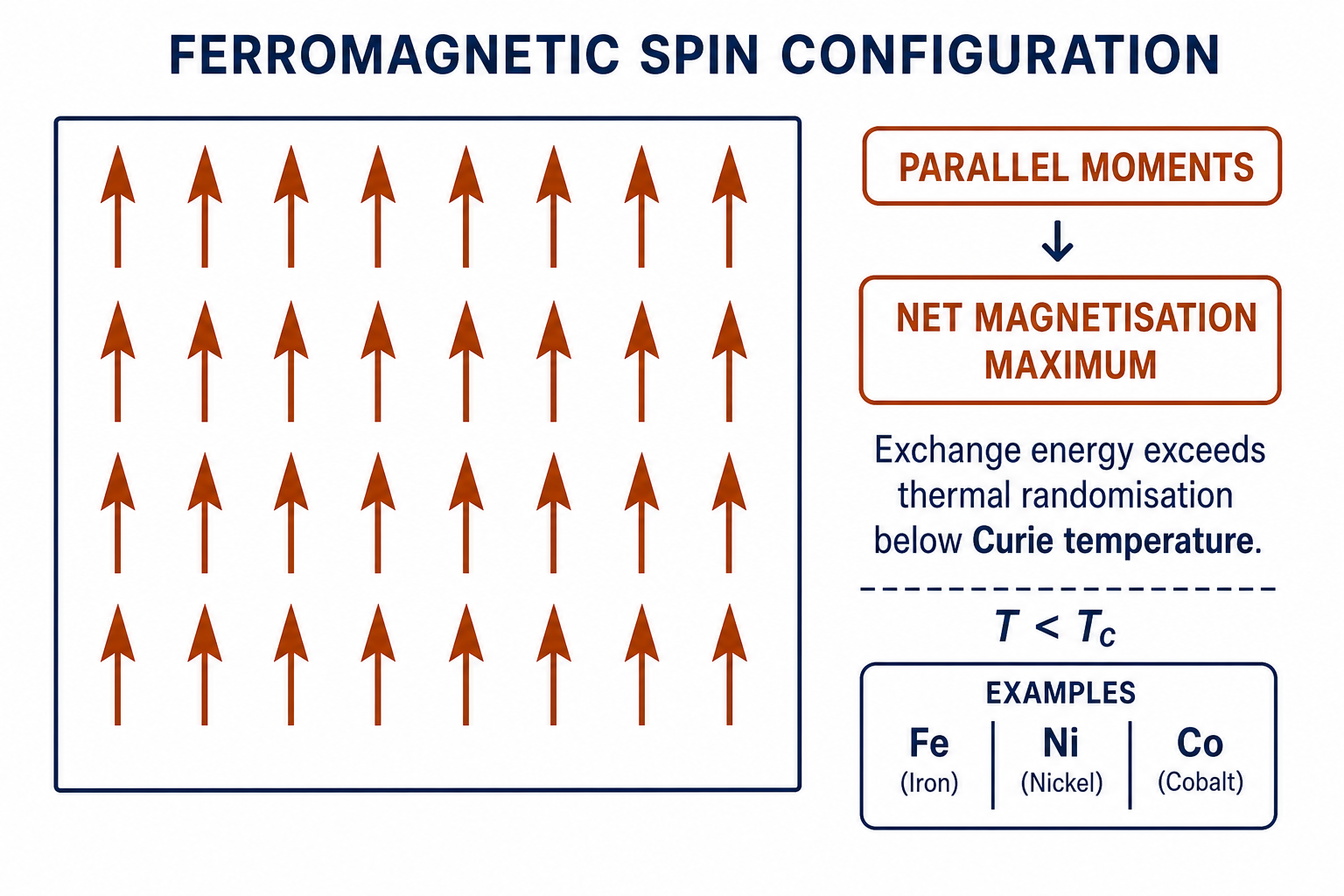
4 Role of Temperature: The Curie Point
Ferromagnetic order is temperature-dependent. As temperature rises, thermal energy increasingly disrupts the exchange-driven alignment. The saturation magnetisation Ms — the maximum achievable magnetisation at a given temperature — decreases continuously until, at the Curie temperature Tc, it drops to zero and the material becomes paramagnetic. The approach to Tc is characterised by thermal energy overwhelming the exchange energy, progressively destroying long-range spin order.
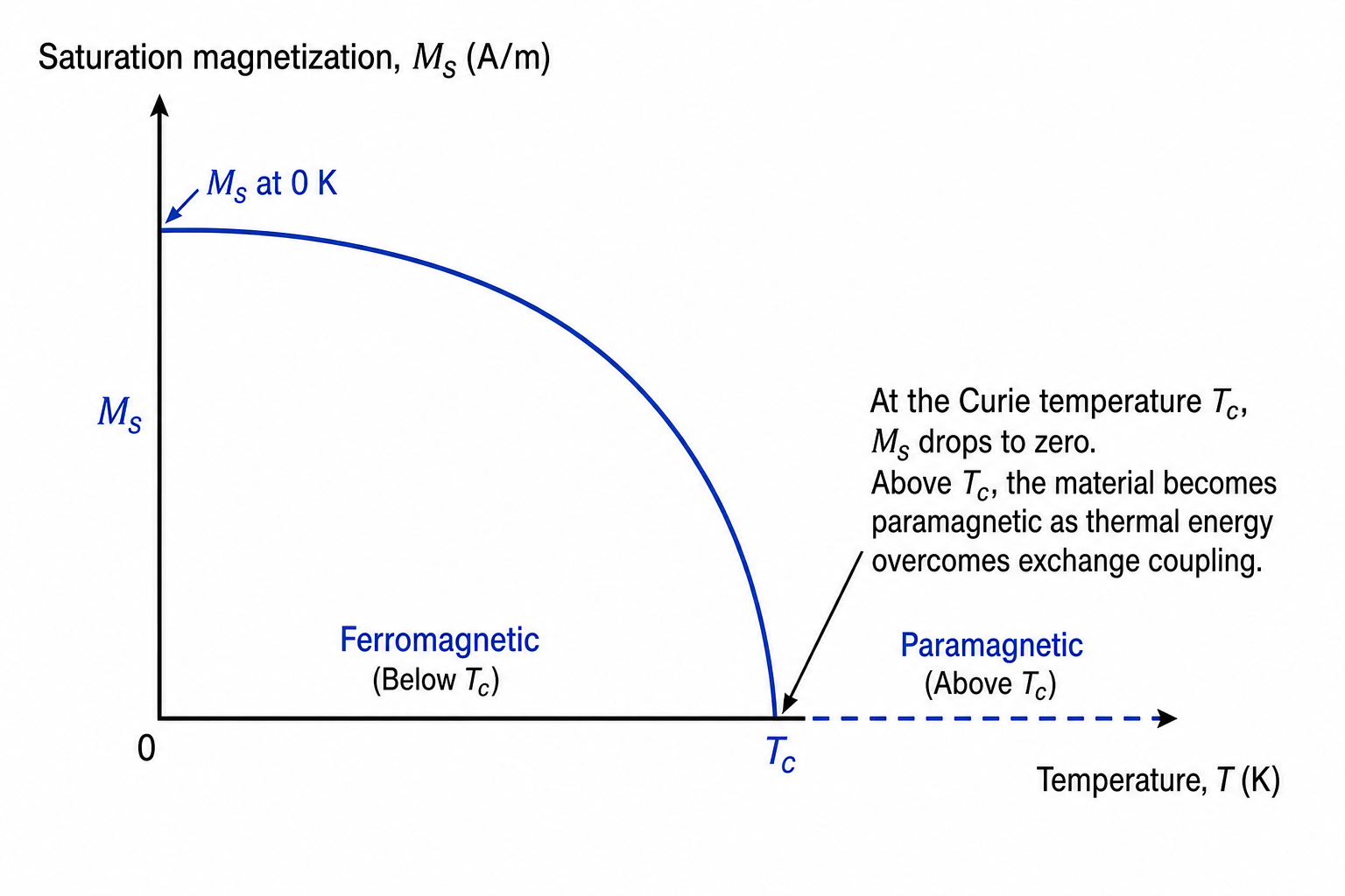
5 The M–H Hysteresis Loop
Magnetic properties are characterised by measuring magnetisation M as a function of applied field H — the M–H or hysteresis loop. Starting from the demagnetised state (point A on the graph), increasing H drives domain growth favourably oriented with the field until saturation magnetisation Ms is reached (point B). Reducing H back to zero leaves a remanent magnetisation Mr slightly less than Ms (point C) — domains do not fully revert. Reversing the field to the coercive field –Hc (point D) is required to reduce magnetisation to zero. Completing the cycle traces the full loop through points E, F, G.
The coercive field Hc measures resistance to demagnetisation. It should be high for applications requiring permanent magnetism (electric motors, magnetic recording media) and low for applications requiring easy switching (strip cards with short life). Magnetic materials are classified by the size and shape of their hysteresis loops: soft magnets (e.g. FeSi) have thin loops with low Hc; hard magnets (e.g. AlNiCo) have fat loops with high Hc.
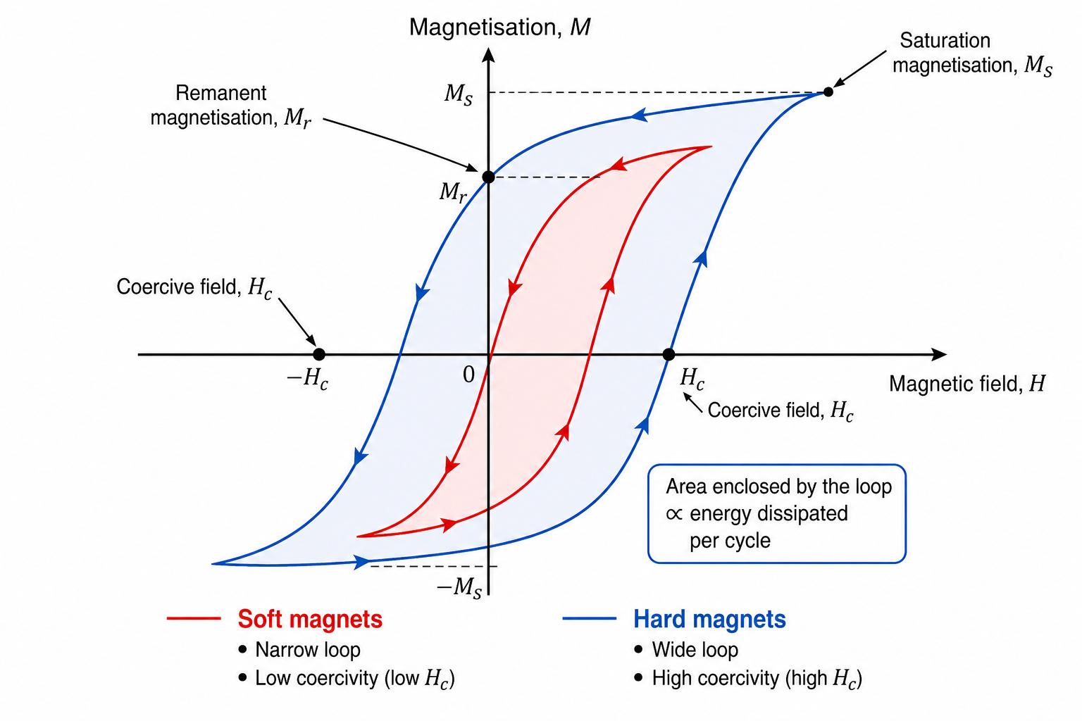
6 Physical Significance of Each Energy Term
Exchange energy (Eexc): The interaction between adjacent atomic magnetic moments. When exchange energy exceeds thermal energy, neighbouring moments align parallel — this is the quantum mechanical origin of ferromagnetism. The exchange field can drive a nearest-neighbour to align in the same direction, sustaining long-range order.
Anisotropy energy (Eani): The energy arising from the tendency of spins to align along specific crystallographic directions called easy axes. In magnetite (Fe3O4), for example, the ⟨111⟩ direction is the easy axis and saturates at much lower applied field than the hard ⟨100⟩ direction. Soft magnetic materials have low anisotropy energy (moments rotate easily); hard magnets have high anisotropy energy (moments resist rotation).
![Left panel: graph of magnetic moment (Am², 0–25) vs applied field H (mT, 0–300) for magnetite. Two curves are shown: a steep blue curve (easy direction, [111]) that saturates rapidly near 50 mT, and a shallower red curve (hard direction, [100]) that requires higher fields to saturate. Right panel: a cubic crystal unit cell with atoms at vertices and face-centres, with vectors labelled Easy ⟨111⟩, Medium ⟨110⟩, and Hard ⟨100⟩ indicating the relative ease of magnetisation along each direction.](nano_images/lec21_fig10.jpg)
Demagnetisation energy (Edem): Related to the dipole character of spins, this energy drives the formation of magnetic domains — regions of uniform magnetisation separated by domain walls. A uniformly magnetised sample has a large external stray field and high magnetostatic energy. Splitting into multiple domains reduces Edem by closing the flux paths inside the material. Two domain morphologies arise: the open domain structure (flux exits the material) and the closure domain structure (flux is channelled internally via 90° domain walls, minimising stray field).
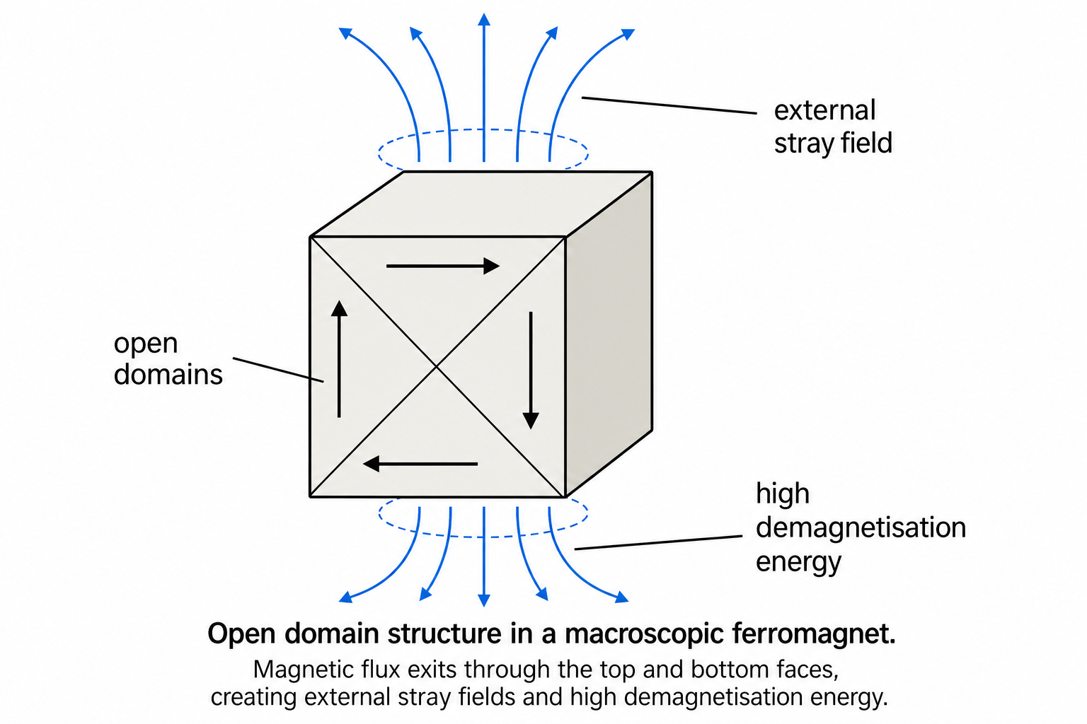
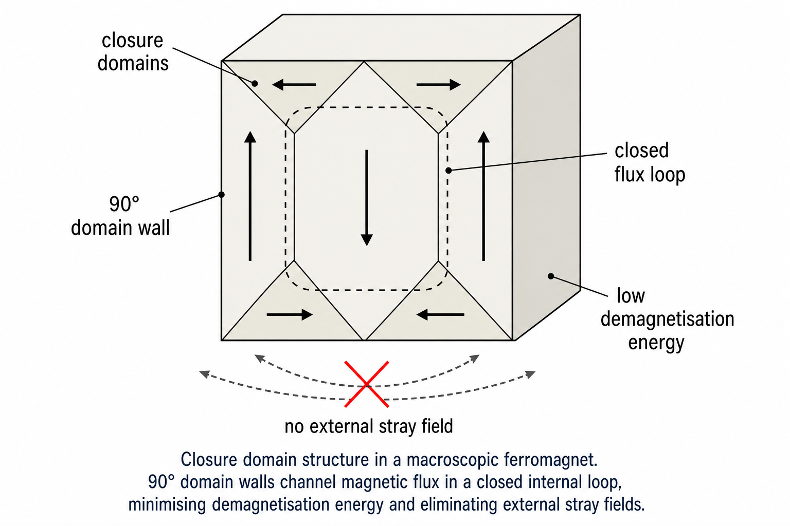
Applied field energy (Eapp): Results from the tendency of spins to align with an applied external field H. As H increases, domain walls move — domains aligned with H grow at the expense of those opposed — until all domains are aligned and saturation magnetisation is reached. Further increase in H produces no additional magnetisation increase.
7 Domain Walls vs Grain Boundaries
A critical distinction: domain walls are not grain boundaries. Grain boundaries are structural interfaces between crystallites with different crystallographic orientations — they are permanent features of the microstructure. Domain walls are magnetic interfaces separating regions of different magnetisation direction — they are dynamic, moving and reforming in response to applied fields. The domain wall width (the transition zone over which spin direction rotates from one domain to the next) is determined by the competition between exchange energy (which favours wide, gradual rotation) and anisotropy energy (which favours abrupt switching at a lattice plane).
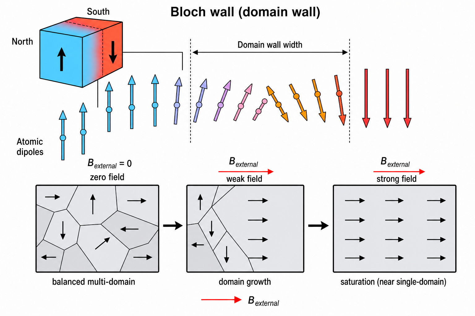
8 Nanoscale Magnetic Behaviour: Critical Grain Size and Superparamagnetism
In nanocrystalline ferromagnetic materials the three energy terms — exchange, anisotropy, and demagnetisation — interact differently from in bulk. For very small particle or grain sizes, the exchange forces become dominant due to strong intergranular coupling, causing spins in neighbouring grains to align collectively, overriding both anisotropy and demagnetising forces. This produces a single-domain state: the entire particle is one uniformly magnetised domain with no internal domain walls.
There is therefore a critical grain size Dcrit below which the material will always be single-domain. For iron this is approximately 14 nm; for cobalt, about 35 nm. Above Dcrit, multi-domain structures form to minimise demagnetisation energy.
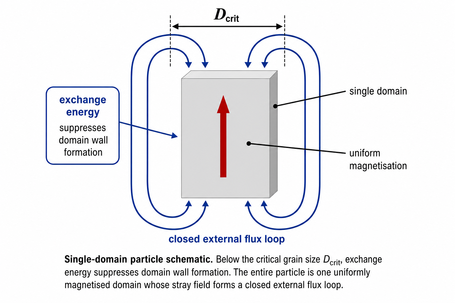
If the particle or grain size is reduced significantly below Dcrit — typically to just a few nanometres — a further effect emerges. The magnetisation of the single domain becomes thermally unstable: random thermal fluctuations carry sufficient energy to spontaneously flip the magnetisation direction. The material appears to have zero coercivity and zero remanence — it is not ferromagnetic but superparamagnetic. Superparamagnetic particles are magnetised in an applied field but retain no magnetisation once the field is removed, just like paramagnets, but with a much larger effective moment per "particle" than a single atom.
9 Effect of Grain Size on Coercive Field
The coercive field Hc — resistance to demagnetisation — has a non-monotonic dependence on particle or grain size. As grain size is reduced from bulk multi-domain (MD) values toward the single-domain diameter Dcrit, Hc increases: single-domain particles have no domain walls to move, so the only demagnetisation mechanism is coherent rotation of the entire spin system, which requires a large reversal field. At Dcrit, Hc reaches a maximum. For grain sizes below Dcrit, further size reduction drives Hc back down rapidly until, at the superparamagnetic diameter Dsp, Hc → 0 as thermal fluctuations dominate.
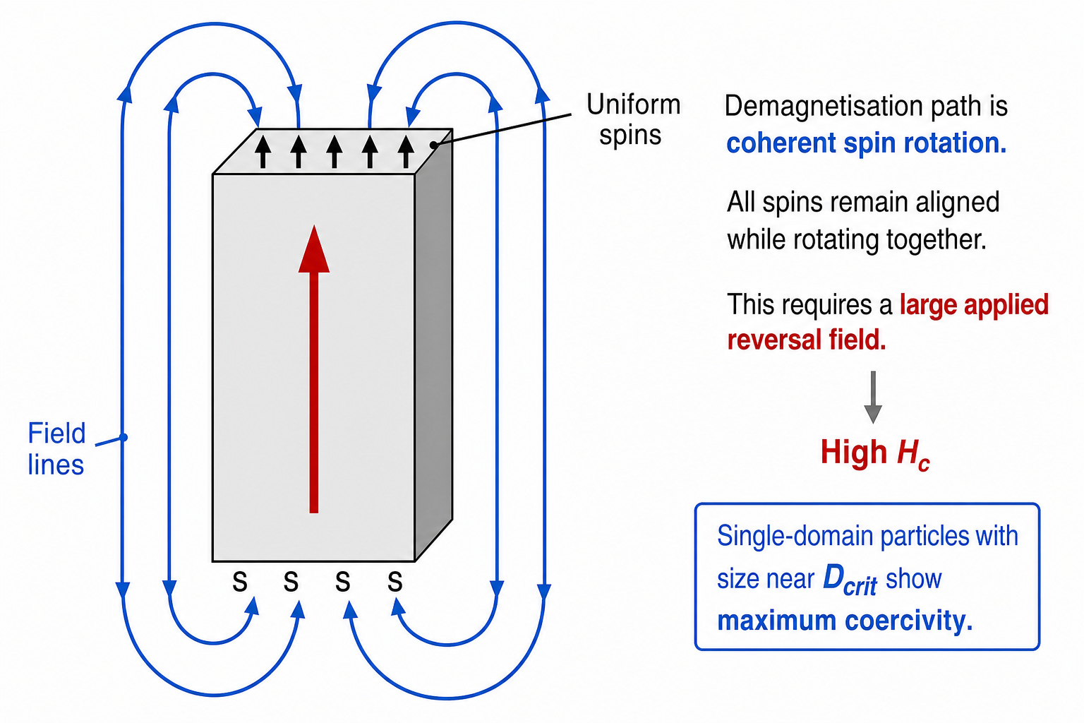
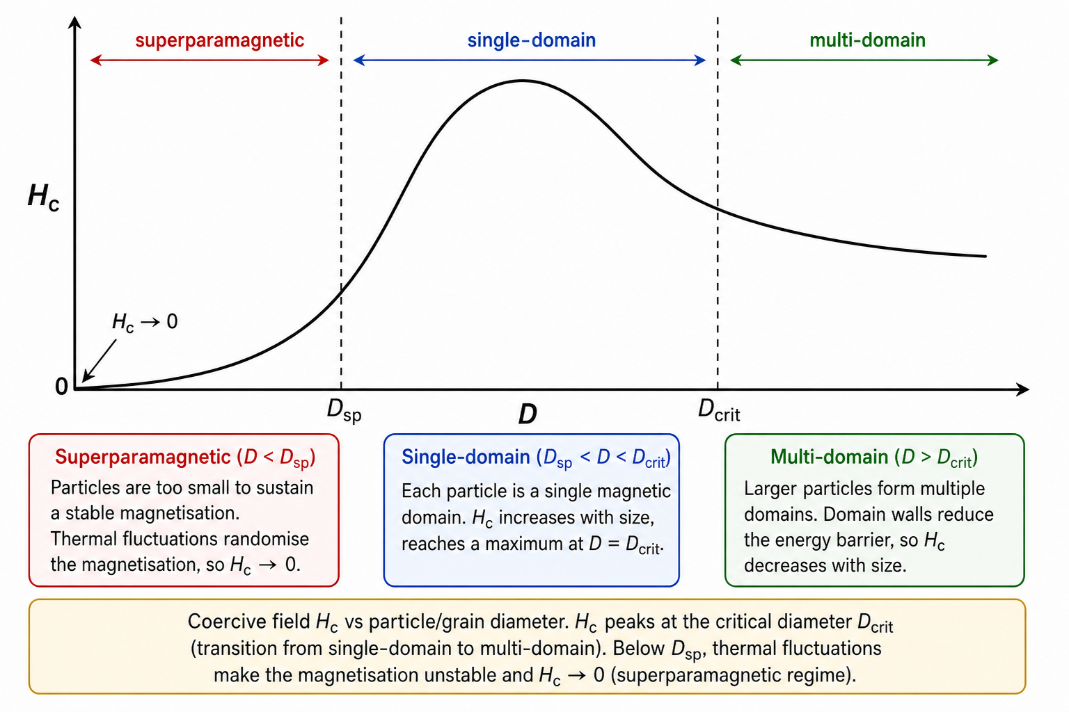
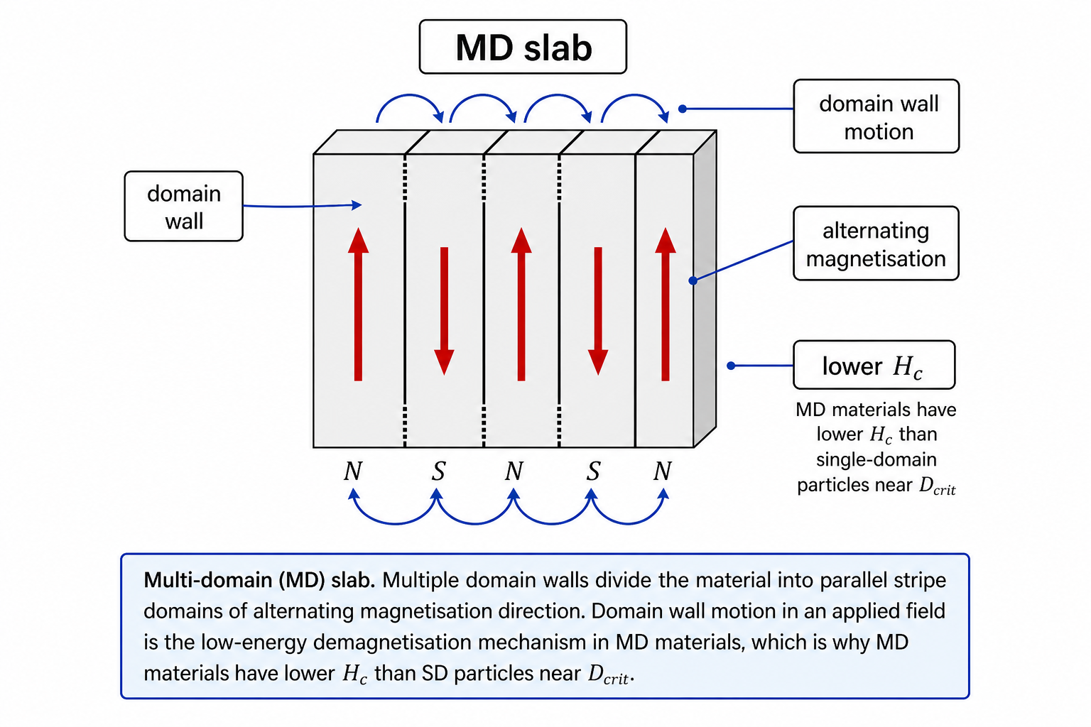
The B–H loop (flux density B vs magnetising force H) is directly related to the M–H loop and shows the same remnant magnetisation and coercivity features. By reducing particle or grain size to the nanoscale, the entire shape of this curve can be engineered — enabling either very soft or very hard magnetic behaviour in the same material system simply by controlling grain size.
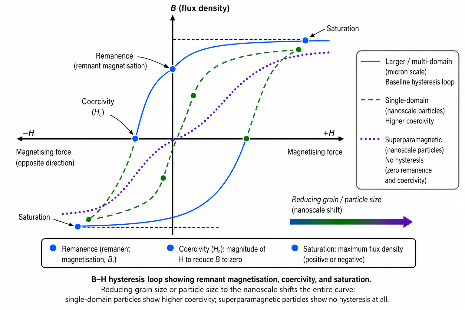
Permanent magnet (high Hc target): grain size should be near Dcrit for single-domain, high-anisotropy material. Coercive force as high as possible.
Soft magnet (low Hc target): low anisotropy energy material; nanoscale amorphous Fe–Ni–Co alloys with 10–15 nm grains can show practically zero hysteresis — ideal for transformer cores and inductors.
Data storage: grain size must be above Dsp (to retain bits) but near Dcrit (for high coercivity and bit stability). Superparamagnetic limit sets a fundamental areal density ceiling.
- Krishnan, K.M., Fundamentals and Applications of Magnetic Materials, Oxford University Press, 2016.
- Knobel, M. et al., Superparamagnetism and other magnetic features in granular materials, J. Nanosci. Nanotechnol., 8(6), 2836–2857, 2008.
- Coey, J.M.D., Magnetism and Magnetic Materials, Cambridge University Press, 2010.
- Cullity, B.D. and Graham, C.D., Introduction to Magnetic Materials, 2nd ed., Wiley-IEEE Press, 2008.
- Total magnetisation energy has four terms: exchange (Eexc), anisotropy (Eani), demagnetisation (Edem), and applied field (Eapp). At the nanoscale, exchange dominates.
- Ferromagnetic materials (Fe, Ni, Co) spontaneously magnetise because exchange energy exceeds thermal randomisation. Above the Curie temperature Tc, they become paramagnetic.
- Magnetic properties are measured by M–H hysteresis loops. Coercive field Hc and remanent magnetisation Mr characterise hard vs soft magnetic behaviour.
- Anisotropy energy drives spins to align along easy crystallographic axes. Hard axes require greater applied field to reach saturation. High Eani → hard magnet; low Eani → soft magnet.
- Demagnetisation energy drives domain formation. Domain walls (dynamic magnetic boundaries) must not be confused with grain boundaries (structural).
- Below the critical grain size Dcrit, exchange coupling produces single-domain particles with maximum Hc. Below Dsp, thermal fluctuations cause superparamagnetism: Hc → 0, zero remanence.
- Nanoscale grain size control enables deliberate engineering of magnetic softness/hardness — with applications in permanent magnets, transformer cores, and magnetic storage media.
Optical Properties of Nanomaterials
How quantum confinement rewrites the rules of light–matter interaction: band gaps, excitons, plasmons, and the size-tuneable colours of quantum dots.
Contents
- Light Absorption in Bulk Semiconductors
- Luminescence and the Blue Shift
- Experimental Evidence: PbSe Nanocrystals
- Excitons: Bound Electron–Hole Pairs
- Exciton Confinement in Nanomaterials
- Confinement and Electronic Structure: 0-D, 1-D, 2-D
- Surface Plasmon Resonance in Metallic Nanomaterials
- Quantum Dots: Size-Programmable Colour
1 Light Absorption in Bulk Semiconductors
In a conventional bulk semiconductor, when an incident photon carries energy greater than the material's band gap, it can promote an electron from the filled valence band up into the empty conduction band. The photon is absorbed in the process, and a positively charged vacancy — a hole — is left behind in the valence band. This is the operating principle of photovoltaic devices.
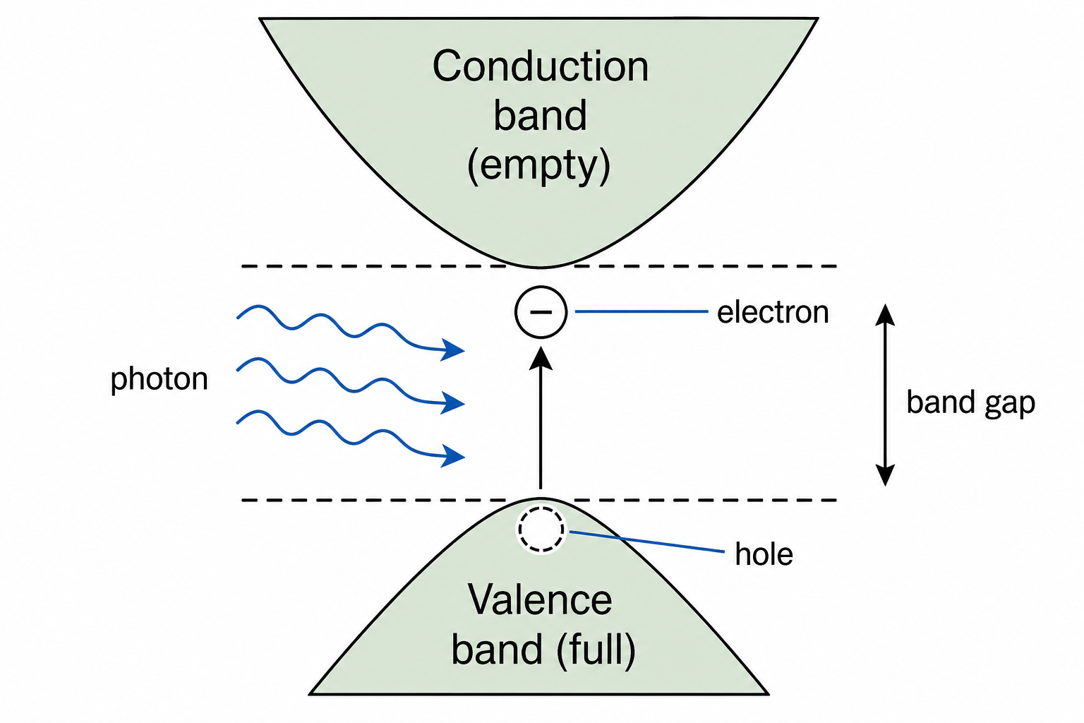
Fig. 22.1 Electron excitation across the band gap of a semiconductor by an incident photon. The electron jumps to the conduction band; a hole is left in the valence band.
The reverse process is equally important: if an electron in the conduction band relaxes back to the valence band and recombines with a hole, a photon is emitted with energy equal to the band gap. This radiative recombination is the basis of light-emitting diodes and semiconductor lasers.
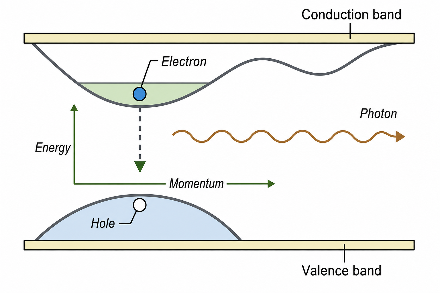
Fig. 22.2 Radiative electron–hole recombination. As the electron falls from the conduction band to the valence band, a photon carrying energy equal to the band gap is emitted.
2 Luminescence and the Blue Shift
When emitted photon energy falls between roughly 1.8 eV and 3.1 eV, the light lies in the visible range — the phenomenon is called luminescence. A key prediction of quantum confinement is that this emission peak shifts toward shorter wavelengths (higher energies) as particle size decreases — a blue shift. Conversely, increasing particle size drives emission toward longer wavelengths — a red shift.
The four-panel diagram below captures the progression clearly. In a three-dimensional bulk solid the density of states D(E) is a smooth, continuous curve — the energy spectrum is a continuum. Confining electrons in one dimension (a quantum well, 2-D) introduces step-like discontinuities. Confining further in two dimensions (a quantum wire, 1-D) produces sharp peaks. In a quantum dot (0-D), confinement in all three spatial dimensions yields fully discrete delta-function-like levels — the limit of maximum quantisation.
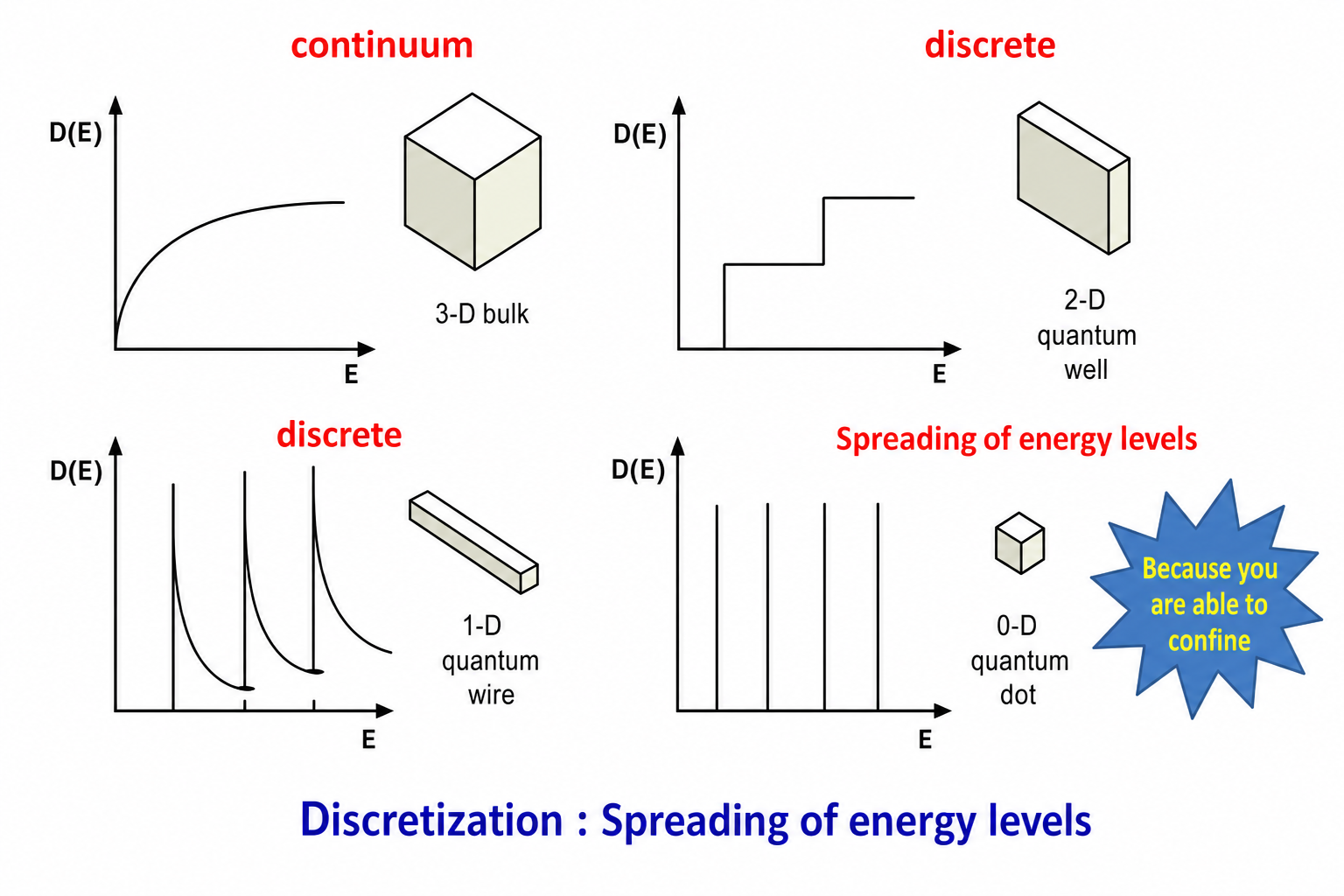
Fig. 22.3 Density-of-states versus energy for bulk (3-D), quantum well (2-D), quantum wire (1-D) and quantum dot (0-D). Reducing dimensionality discretises the spectrum; the 0-D dot has fully separated energy levels.
As the density of states becomes fully quantised, the effective band gap shifts to higher energies and shorter wavelengths. A blue shift is therefore expected in absorption (and emission) spectra as particle size decreases, with a red shift for increasing size.
3 Experimental Evidence: PbSe Nanocrystals
A striking experimental demonstration comes from lead selenide (PbSe) nanocrystals measured at room temperature. The absorption spectra of eight nanocrystal sizes — ranging from 3 nm to 9 nm in diameter — show a clear systematic shift: the smallest particles (a = 3 nm) absorb at the shortest wavelengths (blue end), while the largest (h = 9 nm) absorb furthest into the infrared (red end).
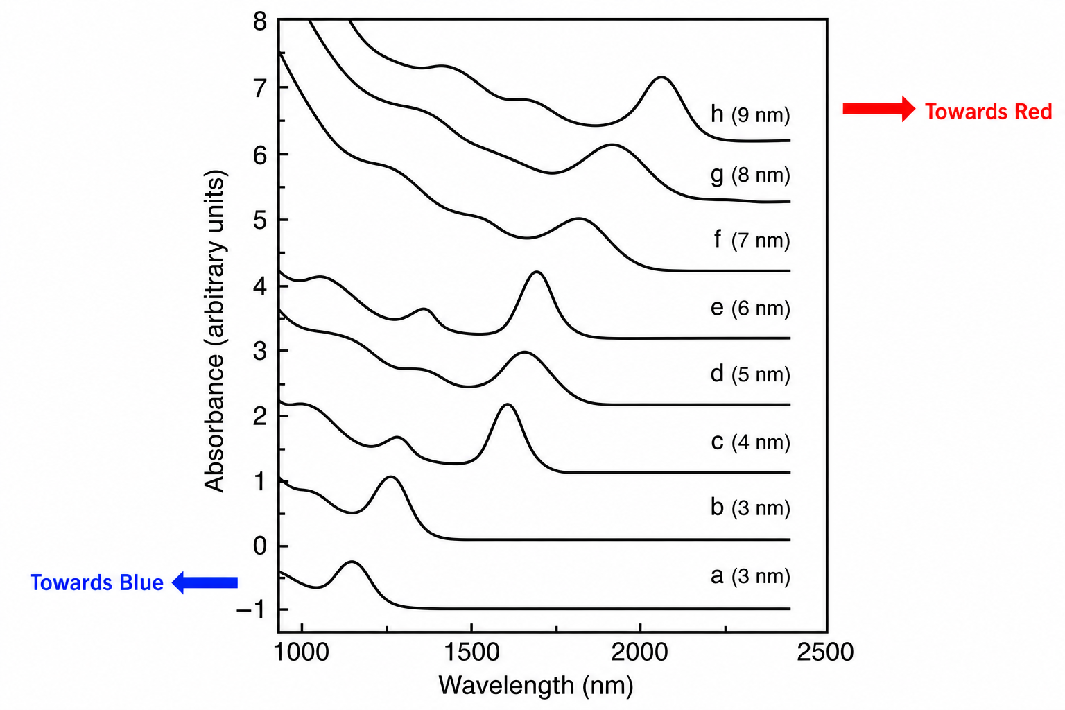
Fig. 22.4 Room-temperature optical absorption spectra of PbSe nanocrystals (diameters 3–9 nm). As particle size increases from (a) to (h), absorption peaks shift from shorter to longer wavelengths (blue → red), confirming quantum confinement theory.
4 Excitons: Bound Electron–Hole Pairs
At low temperatures, bulk semiconductors often display optical absorption just below the energy gap — slightly lower in energy than a free electron–hole pair. This sub-gap absorption arises from the formation of a bound electron–hole pair called an exciton. Unlike a free carrier, the exciton is electrically neutral and can move freely through the material as a mobile quasi-particle.
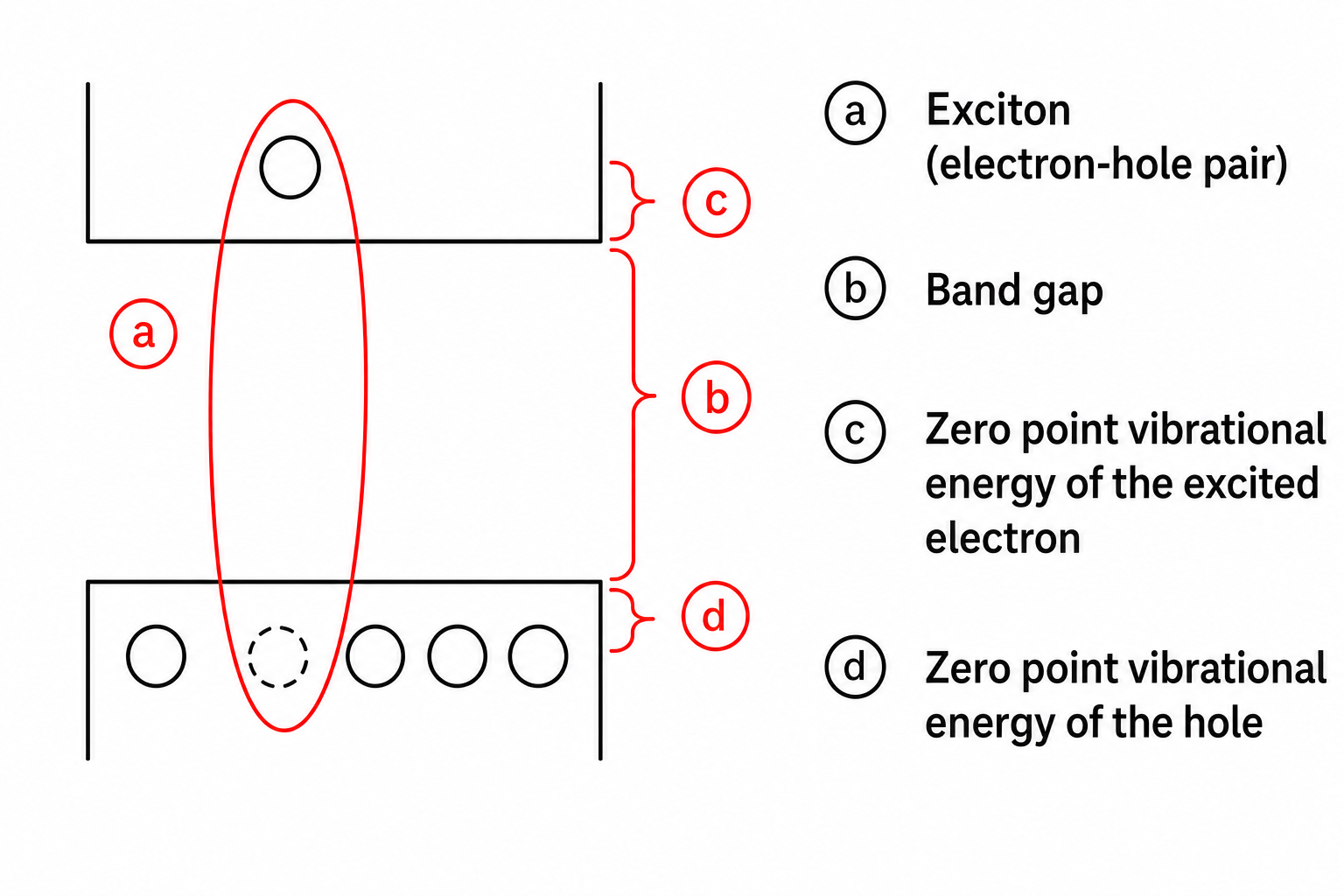
Fig. 22.5 Schematic of an exciton. The electron (minus) occupies a state slightly below the conduction band edge, bound to its hole (plus) by Coulombic attraction. The exciton energy includes zero-point vibrational contributions from both carriers.
The Coulombic attraction between the electron and the hole reduces the energy required to form the pair compared to a fully free electron–hole state at the band gap energy. This pulls the energy levels slightly closer to the conduction band — accounting for the sub-gap absorption seen experimentally.
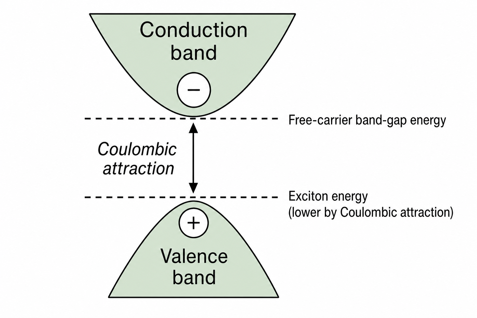
Fig. 22.6 Coulombic attraction between electron and hole in an exciton reduces the effective energy required for pair formation, pulling exciton levels slightly below the free-carrier band-gap energy.
5 Exciton Confinement in Nanomaterials
The spatial extent of an exciton — its exciton radius (or Bohr exciton radius) — is itself a nanoscale quantity. The table below lists exciton diameters and band-gap energies for several common semiconductors. For CdSe, the exciton diameter is ~10.6 nm; for GaAs it is ~28 nm. This means that for a nanomaterial with dimensions comparable to or smaller than these values, the exciton itself is spatially confined — with profound consequences for optical behaviour.
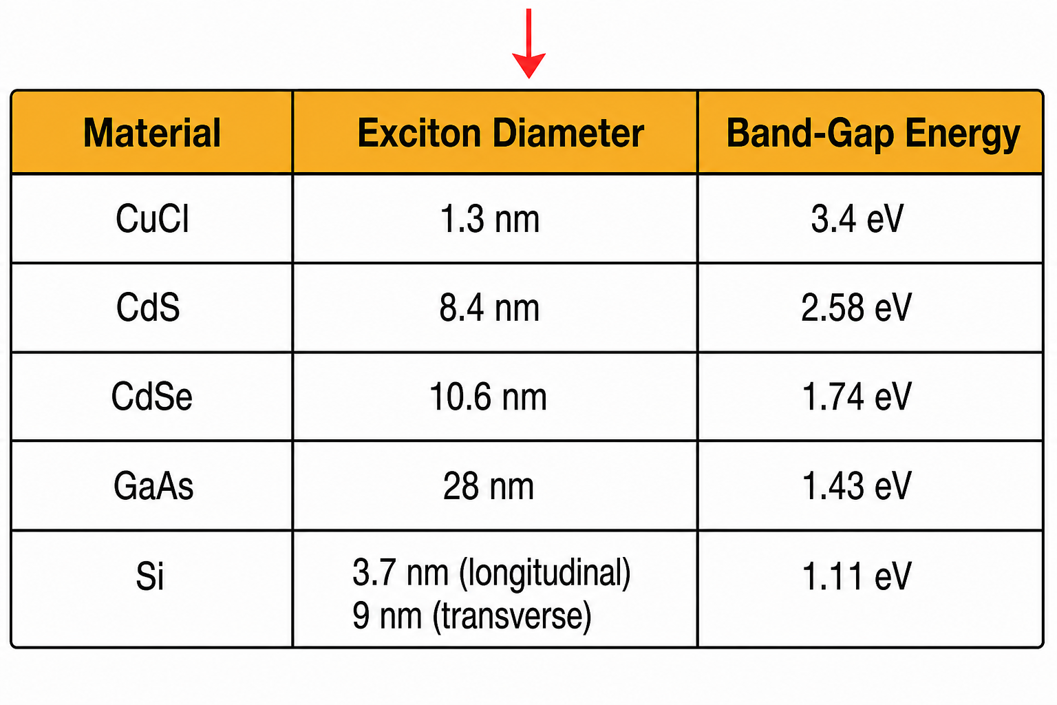
Fig. 22.7 Exciton diameters and band-gap energies for selected semiconductors. Materials with large exciton radii (GaAs, CdSe) experience strong confinement effects at relatively larger nanoparticle sizes.
Two confinement regimes exist. In the weak confinement regime, the nanoparticle dimension is larger than the exciton radius by a few times. Electron and hole are still treated as a correlated pair; Coulombic interaction enhances binding energy and shifts exciton peaks toward the blue. In the strong confinement regime, the particle dimension falls below the exciton radius. Here the electron and hole wavefunctions become uncorrelated — they move independently and the exciton as a bound pair ceases to exist in the classical sense.
6 Confinement and Electronic Structure: 0-D, 1-D, 2-D
Quantum confinement controls not only optical properties but also the fundamental electronic structure of a material. The degree and direction of confinement determines whether electrons are localised or free to move.
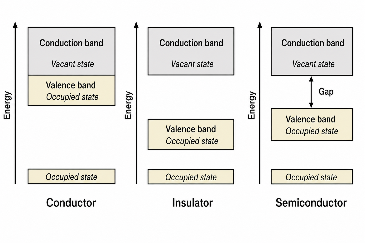
Fig. 22.8 Energy band diagrams for a conductor, insulator, and semiconductor. The semiconductor's small but non-zero gap is what quantum confinement expands in nanomaterials, tuning optical and electronic properties.
In 0-D nanomaterials (quantum dots), the electron is confined in all three spatial dimensions — there is no direction along which it can delocalise. In 1-D nanomaterials (nanowires, nanorods, nanotubes), electrons are confined in two transverse dimensions but are free to delocalise along the long axis. In 2-D nanomaterials (nanosheets, thin films), conduction electrons are confined across the thickness but move freely within the plane. In bulk 3-D materials, electrons are fully delocalised in all directions.
7 Surface Plasmon Resonance in Metallic Nanomaterials
In metallic nanoparticles, a completely different optical mechanism dominates. Plasmons are quantised oscillations of the conduction electron gas. They exist both in the bulk of a metal (bulk plasmons) and at its surface (surface plasmons). Noble metals — gold, silver, copper — are particularly prone to strong surface plasmon resonance because their d-band electronic structures are filled, leaving a highly responsive free-electron gas near the Fermi level.
Surface plasmons have lower frequency than bulk plasmons, allowing them to couple with incoming photons. When photons couple with surface plasmons, alternating regions of positive and negative charge form at the metal surface, generating an electromagnetic wave — a surface plasmon polariton — that is essentially trapped at the interface. This is why gold nanoparticles produce intense, sharply-resonant absorption at visible wavelengths.
The famous Lycurgus Cup (4th century AD, now in the British Museum) exploits this physics. The Roman glassmakers unknowingly embedded gold nanoparticle colloids in the glass matrix. The cup appears green in reflected light but turns a striking red when light is transmitted through it — a direct consequence of the surface plasmon resonance of the embedded gold particles.
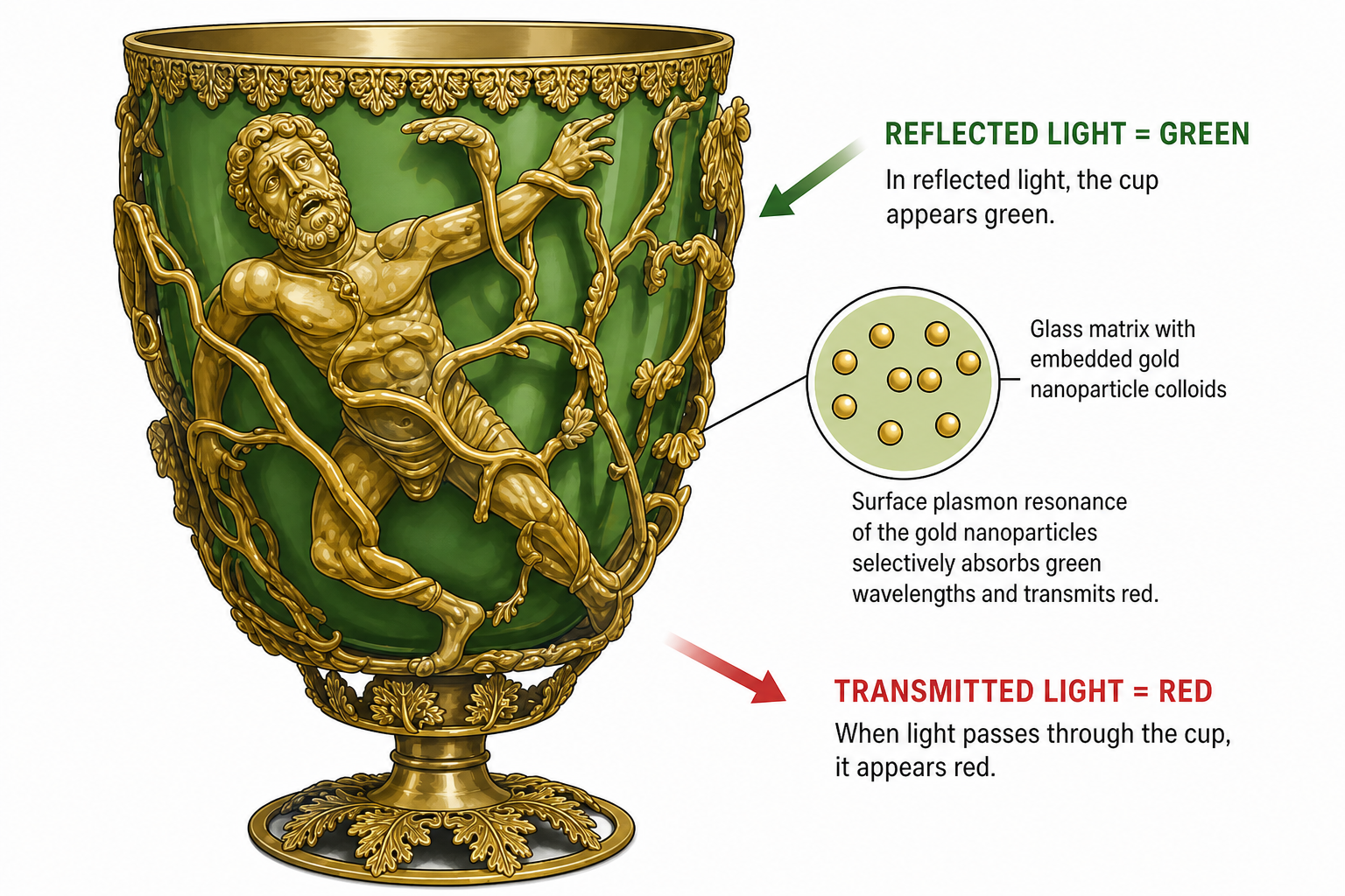
Fig. 22.9 The Lycurgus Cup (4th century AD). Reflected light makes the glass appear green; transmitted light turns it red, due to surface plasmon resonance of embedded gold nanoparticle colloids.
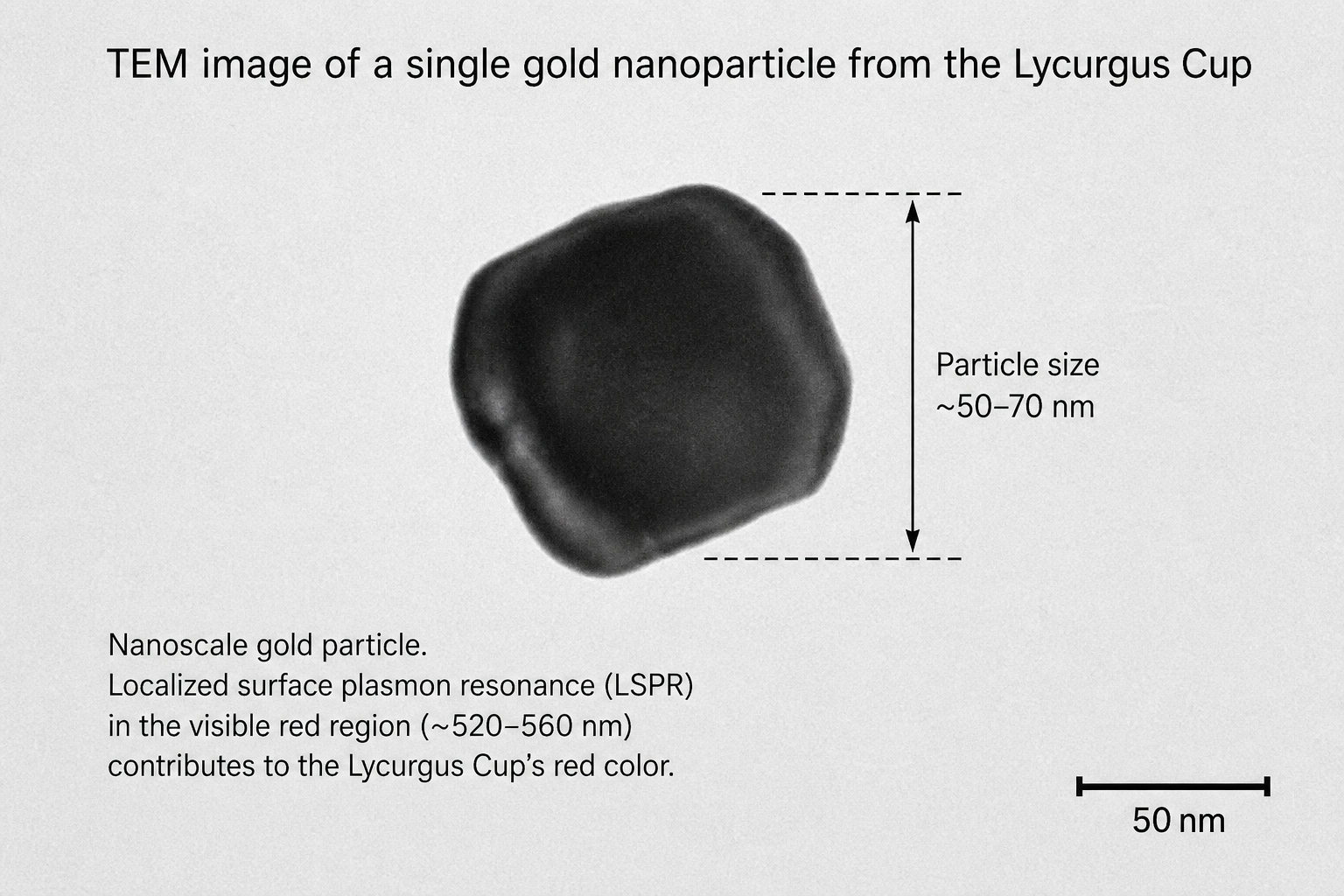
Fig. 22.10 TEM image of a gold nanoparticle from the Lycurgus Cup. The ~50–70 nm particle size places the plasmon resonance squarely in the visible red region of the spectrum.
At smooth metal–air interfaces, momentum conservation prevents direct coupling between free-space photons and surface plasmons. Introducing a thin metal layer between materials with different refractive indices, or using nanostructured metal surfaces, changes the momentum matching condition and enables efficient plasmon excitation — the basis of modern surface plasmon resonance sensors.
8 Quantum Dots: Size-Programmable Colour
Perhaps the most visually compelling demonstration of quantum confinement is the emission of cadmium selenide (CdSe) quantum dots. Because electrons in a quantum dot are confined to widely separated discrete energy levels, the energy of emitted photons — and therefore the colour of emitted light — is a direct function of dot size and shape. Larger dots emit at longer (redder) wavelengths; smaller dots emit at shorter (bluer) wavelengths.
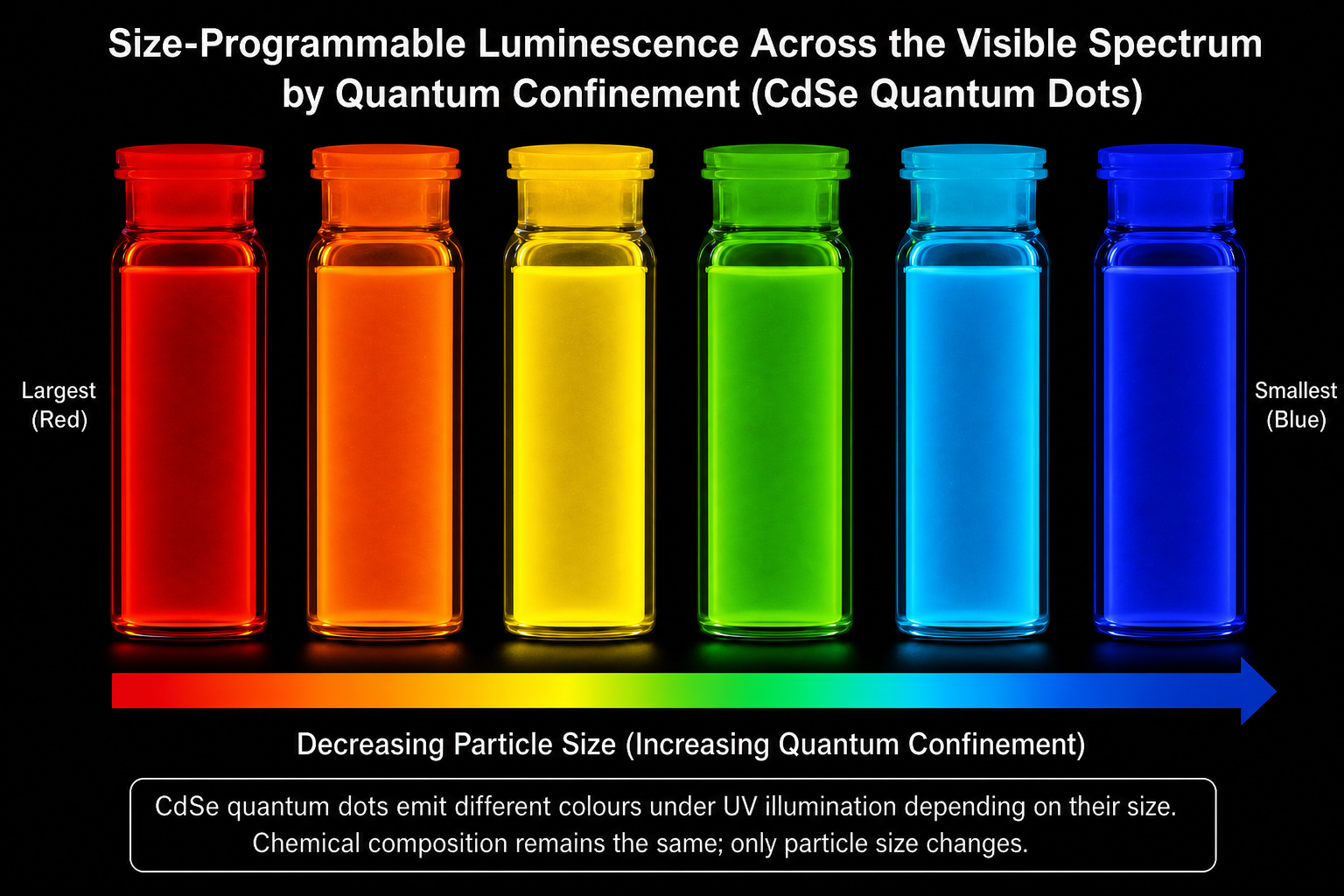
Fig. 22.11 CdSe quantum dot solutions of different sizes and shapes under UV illumination, emitting across the visible spectrum from red (largest) to blue (smallest). The full colour gamut is achieved by quantum confinement alone, with no change in chemical composition.
Key Concepts
- Band gap absorption and radiative recombination in semiconductors are the foundation of photovoltaics and LEDs
- Quantum confinement discretises the density of states and widens the effective band gap, causing a blue shift in absorption and emission as particle size decreases
- PbSe nanocrystal spectra directly demonstrate the size-dependent red/blue shift across 3–9 nm diameters
- Excitons (electron–hole pairs bound by Coulombic attraction) have nanoscale radii; confinement enhances their binding energy and makes them observable at room temperature
- Weak confinement (particle > exciton radius): correlated pair, enhanced binding. Strong confinement (particle < exciton radius): independent electron and hole
- Surface plasmons in noble-metal nanoparticles arise from collective electron oscillations; they produce intense, tuneable visible absorption (as in the Lycurgus Cup)
- CdSe quantum dots emit across the entire visible spectrum by size alone — the definitive demonstration of size-programmable optical properties
Key Takeaways
- Optical properties of nanostructured semiconductors arise from quantum confinement: energy levels discretise and the band gap widens as particle size falls below the exciton Bohr radius, shifting absorption and emission to shorter wavelengths.
- Optical properties of metal nanoparticles arise from surface plasmon resonance: collective conduction-electron oscillations couple to incoming photons, producing intense, size-tuneable absorption peaks in the visible spectrum.
- Both mechanisms are absent in bulk materials — they emerge purely from the nanoscale dimension.
- CdSe quantum dots emit across the entire visible spectrum by size alone, and the Lycurgus Cup demonstrates plasmonic colour in noble-metal nanoparticles thousands of years before the physics was understood.
Biological Applications & Nanotoxicology
How nanoparticles are being harnessed for molecular recognition and diagnostics — and the health and safety questions their unique properties raise.
Contents
- Nanobiotechnology: Two Directions
- Molecular Recognition: Antibodies
- Molecular Recognition: Oligonucleotides and DNA
- Tagging: Nanocrystal–Biomolecule Conjugates
- Application: Colorimetric DNA Analysis
- Engineered Nanoparticles: Properties That Raise Risk Questions
- Potential Risks: Inhalation and Size
- Safe Handling of Nanomaterials
- Toxicological Effects: Summary of Evidence
- Case Study: Nano-Copper vs Micro-Copper Toxicity
1 Nanobiotechnology: Two Directions
Nanobiotechnology sits at the crossroads of materials science and life science. It operates in two complementary directions: using engineered nanostructures as highly sophisticated tools, machines, or probes inside biological systems; and using biological molecules themselves as templates or assembly agents to build nanoscale structures from the bottom up. Both directions are already yielding practical applications in diagnostics, imaging, and targeted drug delivery.
2 Molecular Recognition: Antibodies
The power of nanobiotechnology depends critically on molecular recognition — the ability of one molecule to identify and bind to a specific target with extraordinary selectivity. Biological evolution has produced two classes of molecules that excel at this: antibodies and oligonucleotides.
Antibodies are protein molecules produced by the immune system in response to invading organisms. They can recognise a virus or other antigen as a hostile intruder and bind to it with such precision that other components of the immune system can then destroy the tagged pathogen. The Y-shaped immunoglobulin G (IgG) antibody is the most common class used in biosensing. Its two variable regions at the tips of the Y are the antigen-binding sites — each shaped to lock onto one specific molecular target. The constant region forming the stem of the Y can be coupled to nanoparticle surfaces for signal readout.
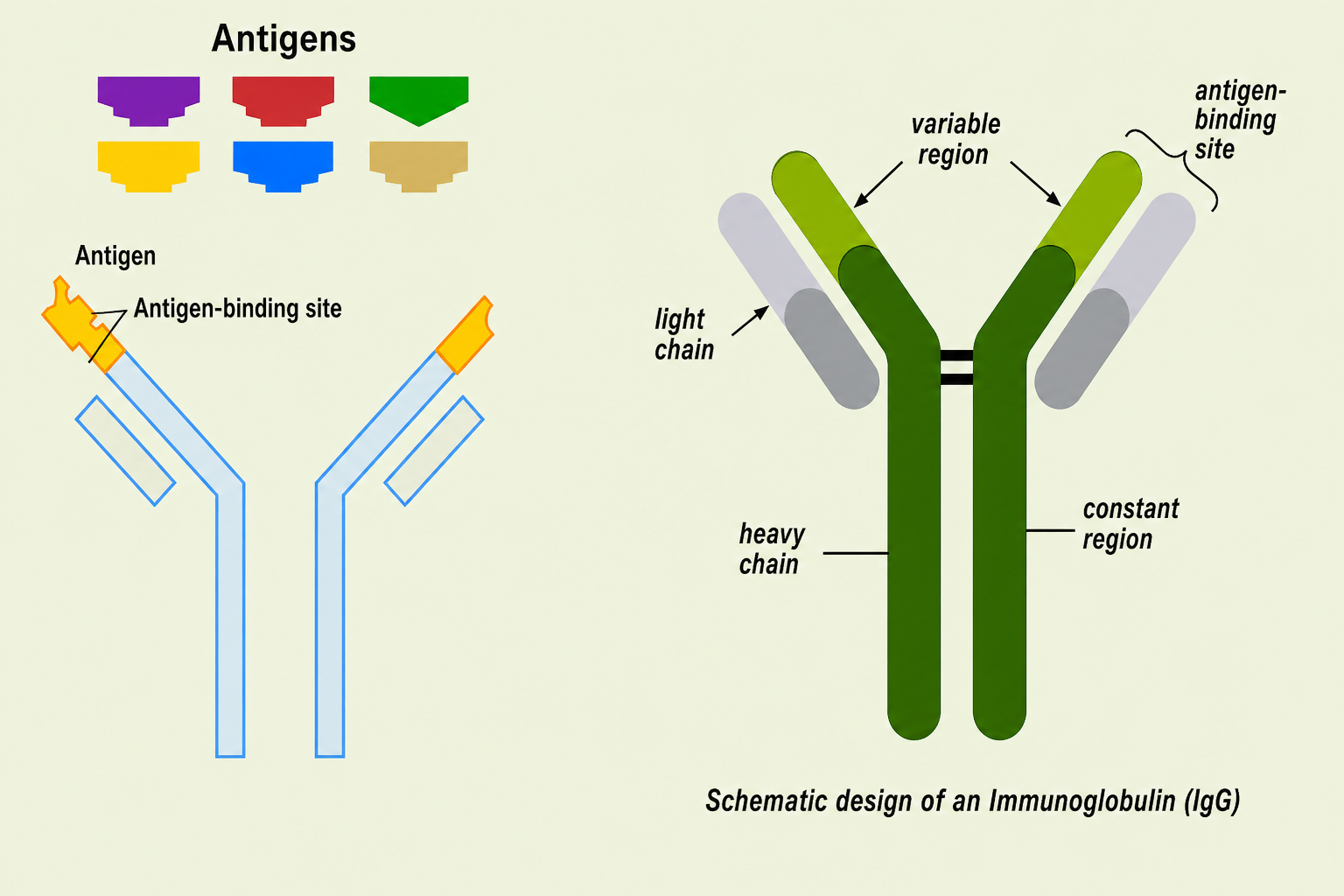
Fig. 23.1 Antibody structure and antigen specificity. The Y-shaped IgG molecule binds a specific antigen at its variable-region tips (antigen-binding sites). Each antigen shape fits only its complementary binding site — the molecular basis of immune specificity.
3 Molecular Recognition: Oligonucleotides and DNA
The second major class of recognition molecule is the oligonucleotide — a short, single-stranded chain of deoxyribonucleic acid (DNA). Each nucleotide in the chain is built from a sugar-phosphate backbone and one of four organic bases: adenine (A), cytosine (C), guanine (G), or thymine (T).
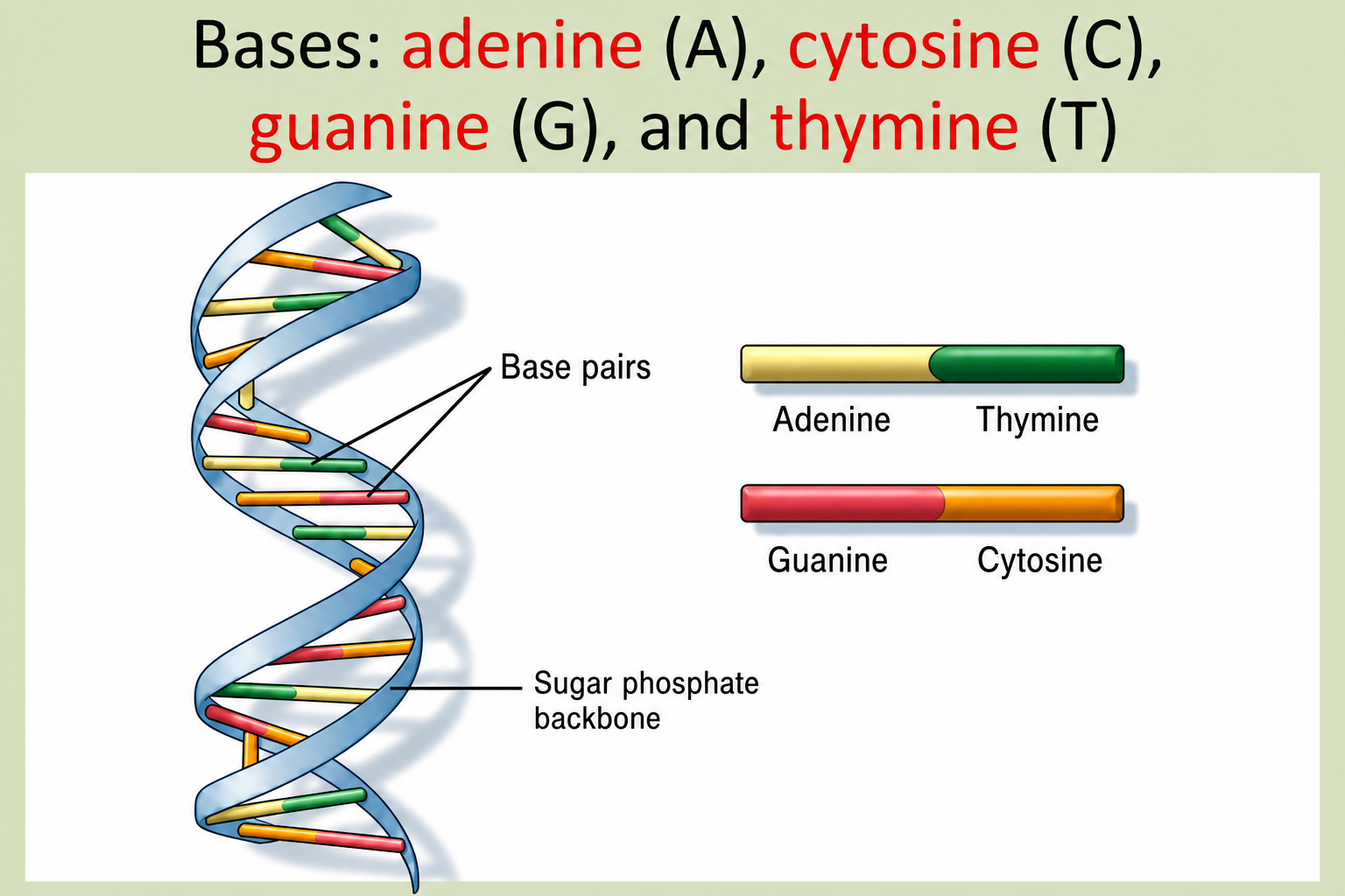
Fig. 23.2 The DNA double helix. The sugar-phosphate backbone forms the rails; the base pairs (A–T and G–C) form the rungs. The sequence of bases uniquely identifies each strand.
The molecular recognition power of oligonucleotides arises from two properties working together. First, every oligonucleotide has a unique identity defined by its base sequence. Second, base pairing is strictly complementary: A only binds to T, and C only binds to G. This means a given oligonucleotide will hybridise only with its exact complementary sequence, making DNA binding highly selective and specific — ideal for detecting particular gene sequences or pathogens.
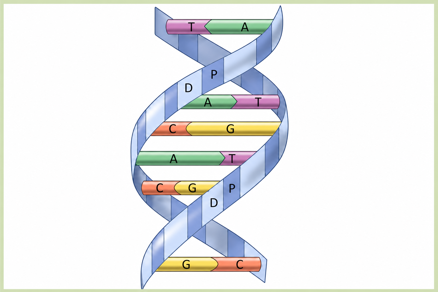
Fig. 23.3 Base-pair specificity in DNA. A pairs only with T; C pairs only with G. This strict complementarity is the basis of oligonucleotide molecular recognition.
4 Tagging: Nanocrystal–Biomolecule Conjugates
In practice, antibodies and oligonucleotides are coupled to nanocrystal surfaces — typically via gold nanoparticles or silanized quantum dots — to create tagged conjugates. When the nanocrystal is attached to a receptor molecule (antibody or oligonucleotide), the resulting conjugate can seek out and bind to a specific biological target, and the nanocrystal provides an optical or electronic signal that reveals the binding event.
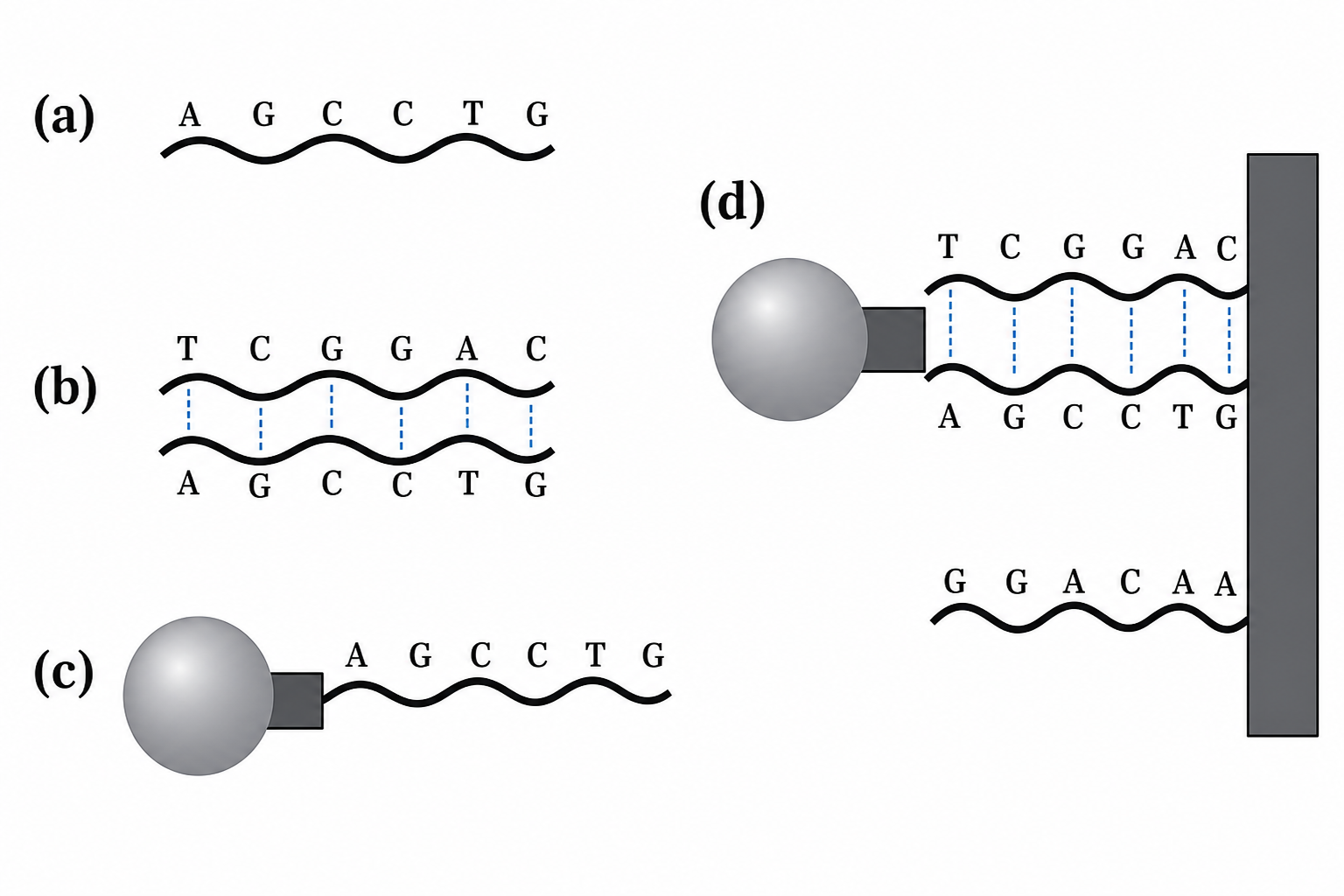
Fig. 23.4 Nanocrystal-oligonucleotide conjugate binding. Steps (a)–(c) show a CdSe/ZnS/Au nanocrystal being conjugated to a six-base oligonucleotide. Step (d) demonstrates sequence-specific surface binding — the conjugate binds only the complementary strand, not mismatched sequences.
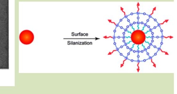
Fig. 23.5 Surface silanization. Silanyl groups (–Si–OH) are attached to the nanocrystal surface, providing coupling handles for further functionalisation with biomolecules.
5 Application: Colorimetric DNA Analysis
One of the most elegant demonstrations of nanocrystal-based molecular recognition is the colorimetric method of DNA analysis. A CdSe/ZnS/Au nanocrystal conjugated to a known six-base oligonucleotide will bind selectively to a surface that displays the complementary sequence — but will not bind to surfaces with different sequences. Because the nanocrystal is optically active (it emits or scatters light at a characteristic wavelength), binding events produce a visible colour change that can be detected without complex instrumentation.
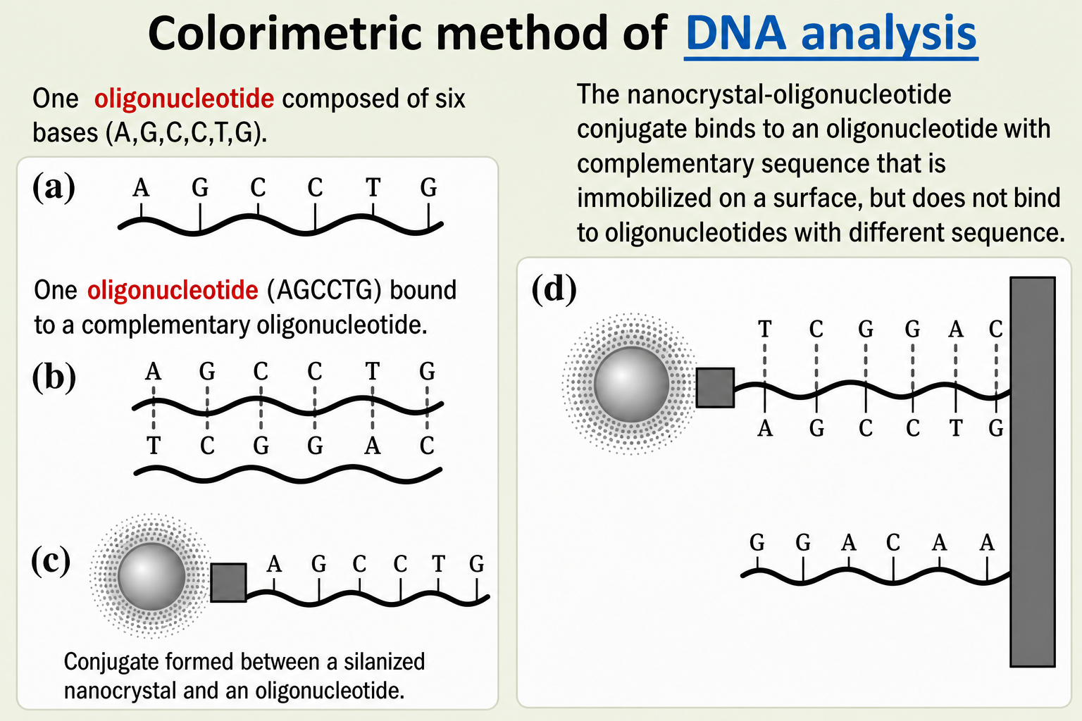
Fig. 23.6 Colorimetric DNA analysis using nanocrystal-oligonucleotide conjugates. The quantum-dot-tagged probe binds only to its complementary sequence on the surface; non-complementary strands are rejected, providing highly specific sequence detection.
6 Engineered Nanoparticles: Properties That Raise Risk Questions
The same properties that make engineered nanoparticles so useful — enormous surface area, quantum-scale dimensions, high chemical reactivity — are precisely the properties that raise health and safety questions. Engineered nanoparticles are intentionally fabricated for their nanoscale properties, and three common examples illustrate the range: fullerene C60 (1 nm diameter, huge surface area), cadmium selenide nanocrystals/quantum dots (6 nm, highly crystalline), and carbon nanotubes (2×100 nm, exceptional mechanical strength).
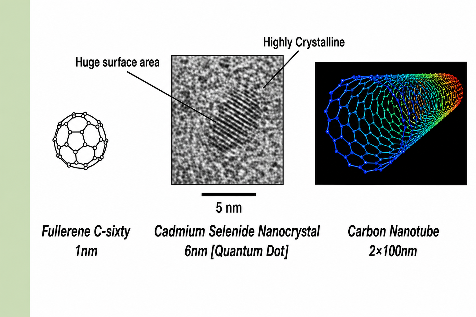
Fig. 23.7 Three archetypal engineered nanoparticles compared at the same scale. Atoms at nanoparticle surfaces experience unsatisfied bonds and are far more reactive than atoms in the bulk — the root cause of both nanoparticle utility and potential toxicity.
A critical point: in nanoparticles, a substantial fraction of all atoms reside at the surface rather than the interior. Surface atoms have incomplete bonding environments and are highly reactive. This drives both the catalytic and biosensing utility of nanoparticles, and their potential to interact chemically with biological tissue in unexpected ways.
7 Potential Risks: Inhalation and Size
A key concern about nanoparticles is their behaviour when inhaled. Particles smaller than 10 µm are respirable — they penetrate deeply enough into the airways to reach the alveolar spaces of the lungs, where gas exchange takes place. Nanoparticles, being orders of magnitude smaller still, can potentially cross the alveolar epithelium, enter the bloodstream, and distribute to distant organs.

Fig. 23.8 The respiratory system showing the alveolar spaces where gas exchange occurs. Sub-10 µm particles reach this region; nanoparticles can penetrate further into the alveolar wall and potentially enter the circulatory system.
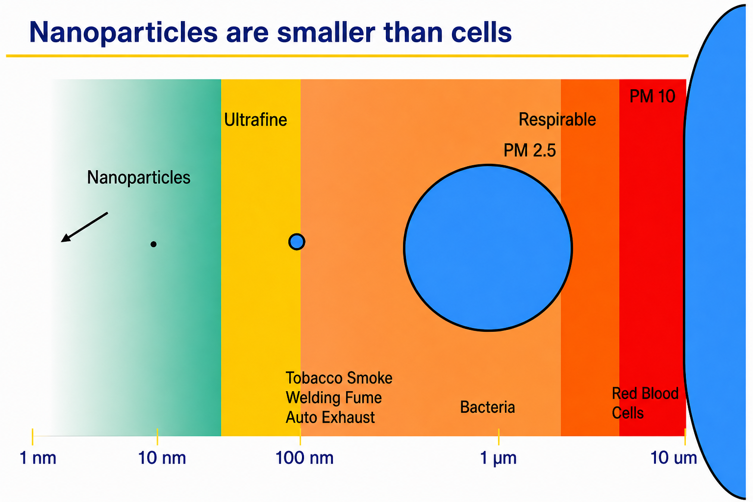
Fig. 23.9 Size relationship of nanoparticles to biological entities and particulate matter classifications. Nanoparticles (1–100 nm) are far smaller than bacteria, red blood cells, and even most environmental fine particles (PM 2.5, PM 10).
8 Safe Handling of Nanomaterials
Because the toxicology of many engineered nanomaterials remains incompletely characterised, precautionary engineering controls are essential. Research on nanomaterial toxicity has increased dramatically. Suggested effects have been observed at the cellular level and in short-term animal tests. Crucially, the biological effects depend on the particle's size, structure, surface substituents, and coatings — not simply its chemical composition. Given this uncertain toxicity profile, recommended controls include exhaust ventilation to remove airborne particles, respiratory protection to prevent inhalation, and dermal barriers to prevent skin exposure.

Fig. 23.10 Nanomaterial safety controls in practice: glove box isolation (top left), PPE for laboratory handling (top right), and full hazmat suit for field-scale particulate exposure (bottom left).
9 Toxicological Effects: Summary of Evidence
The table below summarises the main toxicological concerns identified in early studies, alongside specific experimental examples. The picture that emerges is nuanced: some nanoparticles are cytotoxic in their bare form but can be rendered safe by surface coatings; others cause inflammation or organ translocation that bulk equivalents do not.
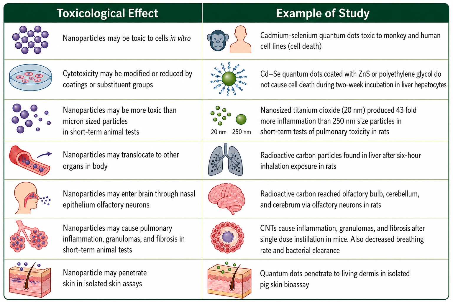
Fig. 23.11 Summary of toxicological effects reported for engineered nanoparticles, with supporting study examples. Effects range from in vitro cytotoxicity to in vivo organ translocation and pulmonary fibrosis.
The cytotoxicity of bare CdSe quantum dots was demonstrated directly in cell-culture studies using monkey and human cell lines. The images below show the nanoparticles themselves (TEM, left), the intense red fluorescence of a CdSe quantum dot suspension under UV excitation (centre), and the primate cell model used in the toxicity assay (right).

Fig. 23.12 Evidence for CdSe quantum dot cytotoxicity. Left: TEM image of CdSe nanoparticle aggregates (scale bar 20 nm). Centre: fluorescence of a CdSe quantum dot solution under UV — the same optical property exploited in biosensing. Right: the primate cell model in which bare CdSe dots caused cell death.
10 Case Study: Nano-Copper vs Micro-Copper Toxicity
A striking illustration of the size-dependent toxicity difference comes from copper particles in gastric juice. When nanosized copper particles (nano-group) are ingested, the stomach acid environment causes them to dissolve rapidly and generate a massive flux of highly toxic cupric ions (Cu²⁺) — far beyond what the body can safely process. In contrast, microsized copper particles (micro-group) dissolve far more slowly under the same conditions, generating only a small quantity of cupric ions that falls within tolerable limits.
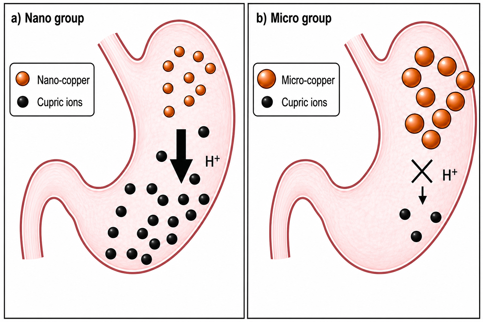
Fig. 23.13 Nano-copper vs micro-copper in gastric juice. Nanoparticles dissolve rapidly in stomach acid, releasing a massive dose of toxic Cu²⁺ ions (a); microsized particles dissolve slowly, releasing only trace amounts (b). The same chemical compound becomes dramatically more toxic at the nanoscale.
11 Characterisation Techniques for Nanoparticles
Transmission Electron Microscopy (TEM) is the most direct tool for characterising individual nanoparticles. In bright-field (BF) imaging, the transmitted beam forms the image — nanoparticles appear as dark objects against a bright background, and the image directly reveals particle size, shape, and degree of agglomeration. Dark-field (DF) imaging uses one or more diffracted beams instead: only grains oriented to satisfy a particular Bragg condition appear bright, so DF is useful for highlighting specific crystal orientations within a polycrystalline sample. High-resolution TEM (HRTEM) resolves the atomic lattice directly — the periodic fringes visible in the image correspond to crystallographic d-spacings, enabling identification of crystal structure and phase without diffraction. Selected Area Electron Diffraction (SAED) from a population of nanoparticles produces ring patterns (rather than the spot patterns of single crystals) because the many randomly oriented crystallites each contribute diffraction spots at all azimuthal angles. The ring radii give the d-spacings, which fingerprint the crystal structure; ring sharpness indicates crystallinity, while diffuse rings signal amorphous or poorly crystalline material.
X-ray Diffraction (XRD) is the standard laboratory method for determining crystal structure, phase composition, and crystallite size in nanoparticle powders. When crystallites are smaller than ~100 nm, the Bragg diffraction peaks broaden measurably beyond the instrumental resolution. This size-dependent broadening is quantified by the Scherrer equation: d = Kλ/(β cosθ), where d is the mean crystallite size, K is a shape factor (typically ~0.9 for spherical particles), λ is the X-ray wavelength, β is the full width at half maximum (FWHM) of the peak in radians (corrected for instrumental broadening), and θ is the Bragg angle. It is important to distinguish crystallite size from particle size: a single nanoparticle may be polycrystalline, composed of multiple crystallites, so the Scherrer size represents the coherently diffracting domain size, which may be smaller than the physical particle. In addition to size broadening, peak shifts away from the expected 2θ positions indicate lattice strain — compressive strain shifts peaks to higher angles (smaller d-spacings) and tensile strain shifts them to lower angles. The Williamson-Hall method separates size and strain contributions to peak broadening by plotting βcosθ versus sinθ.
Dynamic Light Scattering (DLS) measures the size of nanoparticles in suspension by analysing the time-dependent fluctuations in scattered laser light caused by Brownian motion. Smaller particles diffuse faster, producing more rapid intensity fluctuations; the autocorrelation function of the scattered intensity is fitted to extract the translational diffusion coefficient, from which the hydrodynamic radius is calculated via the Stokes-Einstein equation. Crucially, the hydrodynamic radius includes any polymer coating, surfactant layer, or solvation shell on the particle surface — it is therefore always larger than the "hard" core size measured by TEM or XRD. DLS reports a size distribution in the native suspension environment (not dried), which is its principal advantage for colloidal and biological nanoparticle systems. The Z-average size (the intensity-weighted harmonic mean diameter) is the most commonly reported metric, but it is strongly weighted toward larger particles because scattering intensity scales as d6. The polydispersity index (PDI) quantifies the width of the size distribution: PDI < 0.1 indicates a monodisperse sample, 0.1–0.4 is moderately polydisperse, and PDI > 0.4 indicates a broad or multimodal distribution.
BET (Brunauer-Emmett-Teller) surface area analysis measures the specific surface area of a nanoparticle powder by determining the amount of N2 gas adsorbed as a monolayer on the particle surfaces at 77 K. The BET equation is fitted to the adsorption isotherm in the relative pressure range P/P0 = 0.05–0.30 to extract the monolayer capacity, from which the surface area per gram (SA, in m2/g) is calculated using the known cross-sectional area of an adsorbed N2 molecule (0.162 nm2). For non-porous spherical nanoparticles of known density ρ, the equivalent sphere diameter can be estimated as d = 6/(ρ·SA) — a useful cross-check against TEM and XRD sizes. Beyond monolayer analysis, the full adsorption-desorption isotherm reveals information about porosity: the BJH (Barrett-Joyner-Halenda) method analyses the desorption branch using the Kelvin equation to extract the mesopore size distribution (pores in the 2–50 nm range). This is critically important for catalytic nanoparticles, where active sites reside within mesopores, and for drug delivery nanoparticles, where pore size governs drug loading capacity and release kinetics.
Key Concepts
- Nanobiotechnology uses nanostructures as biological probes, and biological molecules to assemble nanostructures
- Antibodies (Y-shaped IgG proteins) and oligonucleotides (single-stranded DNA) provide exquisite molecular recognition via lock-and-key binding
- DNA base pairing is strictly complementary (A–T, C–G), making oligonucleotides highly specific recognition agents
- Nanocrystal–biomolecule conjugates (via gold nanoparticles or silanization) combine recognition specificity with optical signal transduction
- Colorimetric DNA analysis uses quantum-dot-tagged oligonucleotides to detect specific base sequences on surfaces
- Sub-10 µm particles are respirable; nanoparticles can reach alveoli and potentially translocate to distant organs
- Toxicity depends on particle size, structure, surface coatings, and substituents — not composition alone; ZnS or PEG coatings can eliminate CdSe cytotoxicity
- Nano-copper dissolves far faster in gastric acid than micro-copper, generating toxic Cu²⁺ ion levels far exceeding those from equivalent bulk material
- Controls: exhaust ventilation, respiratory protection, dermal barriers when working with nanomaterials
Key Takeaways
- Nanoparticles serve as biosensing tags by coupling quantum dots to antibodies or DNA — quantum dot fluorescence provides optical readout; antibody/oligonucleotide specificity provides molecular recognition.
- The same nanoscale properties enabling applications — high surface area, quantum confinement, chemical reactivity — also create safety concerns.
- Evidence shows nanoparticles can be cytotoxic, cause pulmonary inflammation, translocate to remote organs, and penetrate skin; toxicity is strongly size- and surface-chemistry-dependent rather than composition-dependent alone.
Field Ion Microscopy & Nanotoxicology
Atomic-resolution imaging with field ion microscopy, the 3D atom probe technique, and a thorough treatment of health and environmental hazards posed by engineered nanomaterials.
Contents
1 Field Ion Microscopy — Principles
Field ion microscopy (FIM) is one of the most powerful surface characterisation tools ever devised, capable of resolving individual atoms at a specimen surface. Unlike conventional microscopes, which rely on electrons or photons as the imaging probe, FIM uses ionised gas atoms. This distinction is fundamental: because ions are far heavier than electrons, their de Broglie wavelength is negligibly small, and the resolution of the instrument is limited not by diffraction but by the physical size of the ionisation zone above each surface atom — on the order of interatomic dimensions, roughly 2–5 Å.
The specimen is a fine needle with a tip radius of just 5–50 nm, prepared by electropolishing a metal wire until the apex reaches near-atomic sharpness. It is mounted inside a cryogenically cooled ultra-high-vacuum chamber and held at temperatures between 20 K and 100 K. Cooling is essential: at cryogenic temperatures, thermal vibrations of surface atoms are suppressed to the point where individual atom positions become stable and resolvable. A large positive voltage of 5–20 kV is then applied to the tip, generating an electric field at the apex in the range of 1010 V m−1.
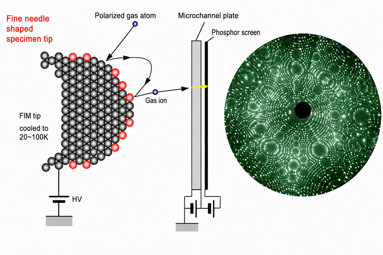
Fig. 24.1 FIM schematic and resulting image. Gas atoms polarised at the tip are ionised, repelled, and projected onto a phosphor screen, mapping atomic positions on the tip surface.
The chamber is backfilled with an imaging gas — helium or neon at pressures of around 10−3 Pa. These noble gas atoms are weakly adsorbed on the tip surface and polarised by the intense electric field. At protruding surface atoms, where the field is locally strongest, adsorbed gas atoms are field-ionised: the outermost electron tunnels from the gas atom into the tip, converting the neutral atom into a positive ion. The resulting ion is immediately repelled by the positively biased tip and accelerated radially outward toward a microchannel-plate detector backed by a phosphor screen. Each bright spot on the screen corresponds to a position above one atom on the tip surface. The magnification is simply the ratio of the screen radius to the tip radius — typically of the order of 106 — and the full hemispherical surface of the tip is imaged simultaneously.
2 The FIM Image — Reading Atomic Structure
The resulting image is a projection of the tip surface in which every visible spot marks a single atom. Because the tip is approximately hemispherical, the image represents a stereographic-like projection of all the crystallographic planes accessible on the surface. Low-index planes — (110), (100), (111) and so on — appear as dark rings or discs at the centre of concentric arcs of bright spots corresponding to terrace edges, while high-index regions between the poles are densely populated with spots. The overall pattern is thus a map of the crystal symmetry, and trained microscopists can immediately identify the crystallographic orientation and detect any departure from perfection.
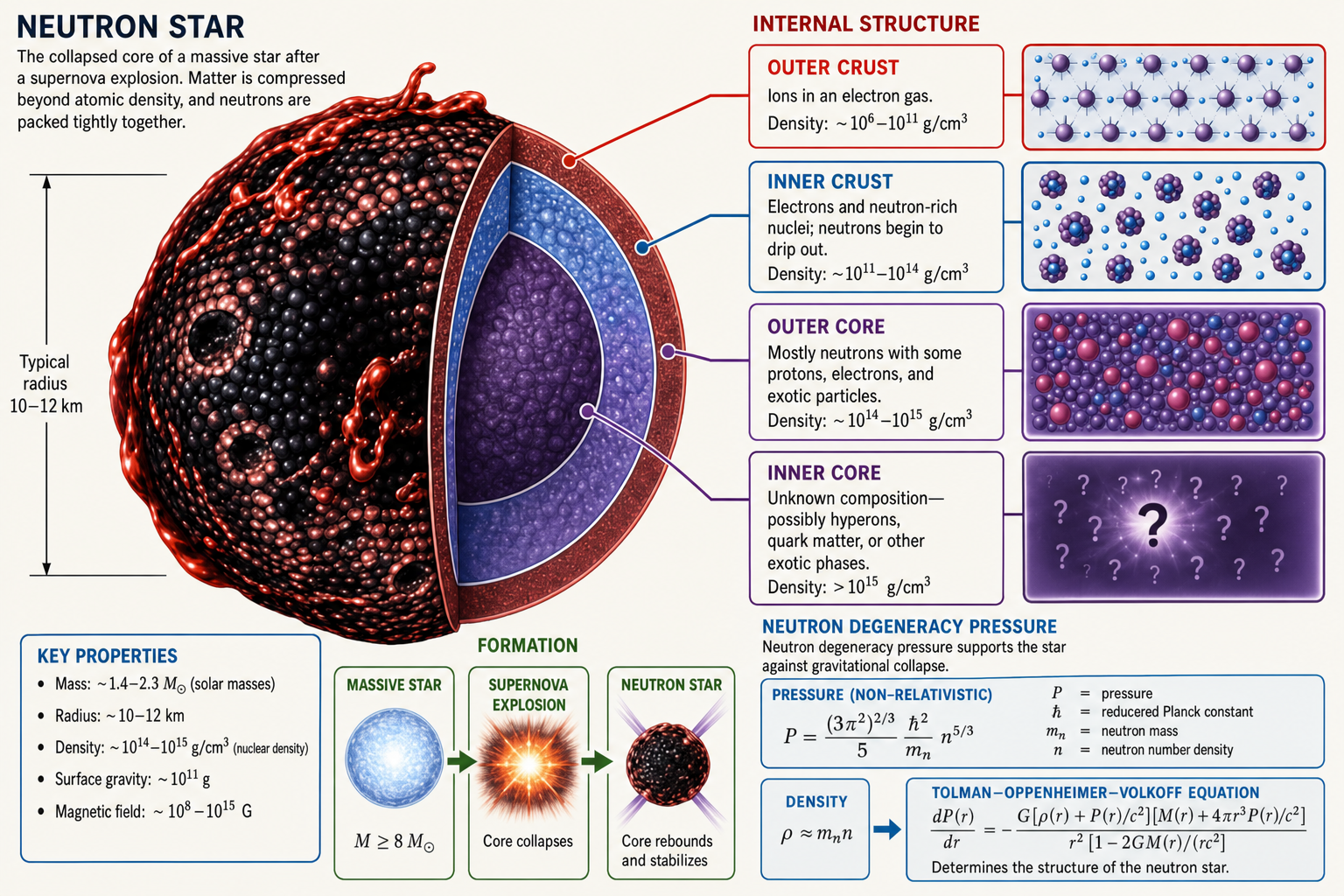
Fig. 24.2 FIM image of a sharp tungsten needle. Each bright point is a single surface atom. The concentric ring structure reflects the stepped terraces of the hemispherical tip.
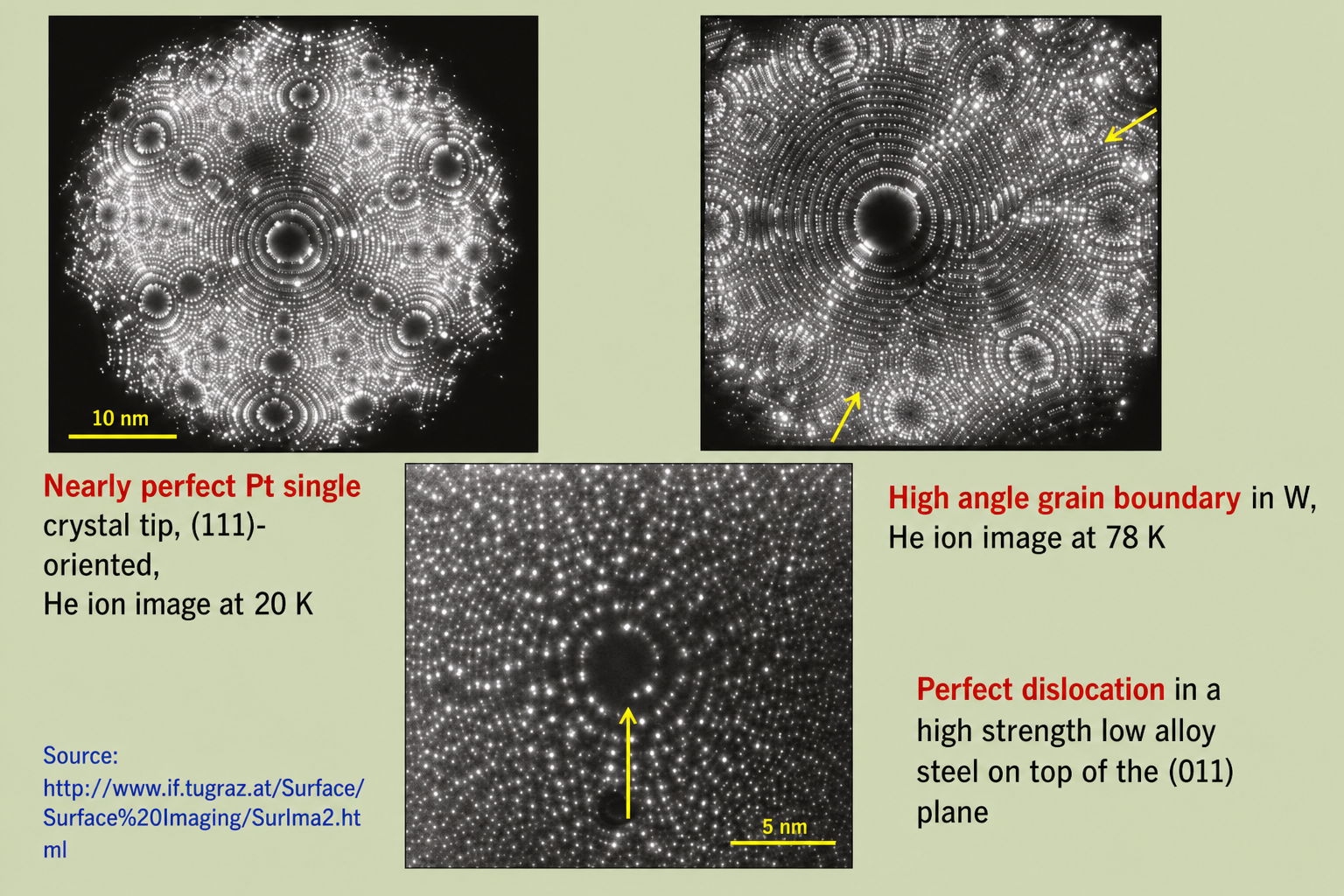
Fig. 24.3 Representative FIM images. Left: nearly perfect Pt single crystal tip, (111)-oriented, He ion image at 20 K. Upper right: high-angle grain boundary in W, He ion image at 78 K. Lower centre: perfect dislocation in high-strength low-alloy steel on the (011) plane, 5 nm scale bar.
At room temperature, thermal vibration displaces surface atoms by ~0.1–0.2 Å rms, blurring the ion emission spots and preventing atomic resolution. Cooling to 20–100 K reduces this motion by an order of magnitude, making individual atom positions stable enough to be resolved.
Defects in the crystal structure are directly visible in FIM images as local departures from the regular spot pattern. Grain boundaries appear as abrupt steps or disorientations across the image; dislocations emerge at the surface as characteristic spiral or split-ring contrast features; vacancies and adatoms show up as missing or extra bright spots. This makes FIM uniquely powerful for studying the atomic-scale structure of crystalline defects under controlled conditions.
FIM does have notable limitations. First, the specimen geometry is highly constrained — only materials that can withstand the enormous electric field at the tip without evaporating are suitable; this restricts the method primarily to refractory metals (W, Mo, Pt, Ir, Rh, Fe, Ni) and some alloys. Second, specimen preparation and surface contamination control are demanding. Third, the small volume sampled (a hemisphere of radius 5–50 nm) means the technique sees only a tiny fraction of any bulk material.
3 Field Desorption and the 3D Atom Probe
If the electric field at the tip is increased beyond the imaging threshold, surface atoms themselves become field-ionised and desorbed from the tip as positive ions — a process called field evaporation or field desorption. This can be exploited in several ways: the surface can be cleaned by removing contaminant atoms layer by layer; the tip can be sectioned into depth by sequential field evaporation; and, most powerfully, the desorbed ions can be directed into a time-of-flight mass spectrometer to identify their chemical identity. This combination of FIM imaging with mass spectrometric analysis of field-desorbed ions constitutes the atom probe technique.
In the modern three-dimensional atom probe (3DAP), every atom that is field-evaporated from the tip is detected with its mass-to-charge ratio (giving elemental identity) and its position on the detector (giving lateral position), while the sequence of evaporation events provides depth information. By accumulating data from tens of millions of evaporation events, the instrument reconstructs the three-dimensional elemental distribution within the analysed volume atom by atom. The result is a point cloud in which each atom is colour-coded by element, with spatial resolution of ~0.1–0.5 nm in depth and ~0.3–0.5 nm laterally over a volume of typically 100 × 100 × 300 nm.
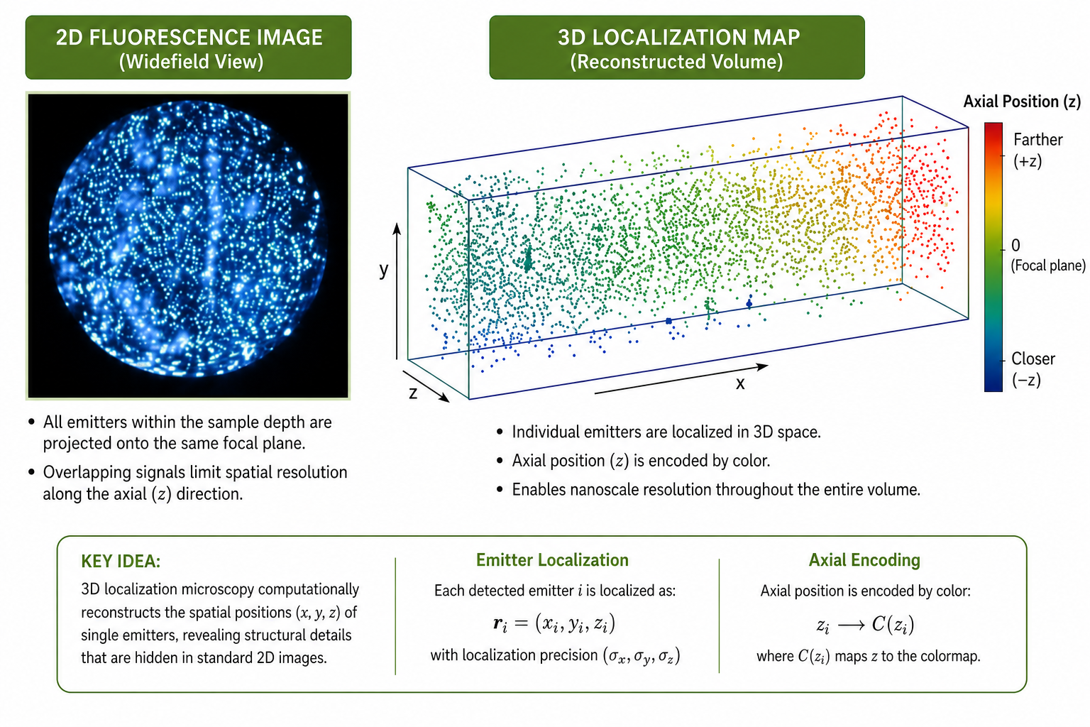
Fig. 24.4 FIM used as a 3D atom probe. Left: Ne ion image of precipitation in tool steel, 40 nm diameter area imaged at 40 K. Right: 3D reconstruction of atom probe data from the matrix of a tool steel — a 10 nm diameter, 200-atomic-layer-deep elemental map showing solute atom positions.
The 3DAP is uniquely valuable for nanomaterials characterisation. It can map the elemental distribution within nanoparticles, resolve solute segregation at grain boundaries with sub-nanometre precision, track precipitate nucleation and growth atom by atom, and reveal clustering in amorphous films. No other technique provides simultaneous elemental sensitivity and spatial resolution at this scale.
4 Environment and Health Issues — The Toxicological Foundation
The same surface-area enhancement that makes nanomaterials so attractive for catalysis, drug delivery, and energy storage also creates potential hazards. Because the surface-to-volume ratio scales inversely with particle radius, a nanomaterial may present orders of magnitude more reactive surface per unit mass than its bulk counterpart. Since surface atoms are coordinatively unsaturated — they have unfulfilled chemical bonds — nanoparticles are intrinsically more reactive toward biological molecules, cell membranes, and atmospheric species. This principle is captured in the concept of dosage versus surface area: the physiologically relevant dose of a nanomaterial is better expressed in terms of surface area (m² per lung, per kg body weight) than in mass, because reactivity scales with surface rather than mass.
The Renaissance physician Paracelsus observed that "poison is in everything, and no thing is without poison — the dosage makes it either a poison or a remedy." This centuries-old principle applies with particular force to nanomaterials, where dose expressed in mass may dramatically underestimate biological reactivity compared with dose expressed in surface area or particle number.
Several distinct mechanisms by which nanoparticles can be more toxic than equivalent bulk particles have been identified. First, intrinsic chemical reactivity is enhanced: a platinum nanoparticle of 5 nm diameter has approximately 30% of its atoms at the surface, compared with a fraction of a percent for a 1 μm particle — each surface atom is a potential active site for unwanted chemistry in biological environments. Second, the small size of nanoparticles — substantially smaller than many human cell types — enables them to cross biological barriers that would be impassable to larger particles, penetrating the cell membrane, entering the nucleus, crossing the blood–brain barrier, or translocating from the lung epithelium into the bloodstream. Third, the surface chemistry of nanoparticles can be tuned by attaching functional groups or ligands, which offers a design handle for minimising toxicity, but also means that different surface functionalisations of nominally the same material may exhibit dramatically different biological interactions.
Nanomaterials currently in commerce span a wide range of applications, from passive to active. Passive applications — in which the nanoparticle does not interact specifically with biological targets — include cosmetics formulated with titanium dioxide or zinc oxide nanoparticles, silver-based antimicrobial products, and carbon nanotube-reinforced sporting goods. Active applications, in which designed nanomaterials interact with specific biological targets, include dendrimer-based anticancer drug carriers engineered to seek out cancer cells, bind selectively, and release a therapeutic payload locally, and iron-oxide nanoparticles for magnetic resonance imaging contrast enhancement.
5 Specific Nanotoxicological Concerns
Several specific nanotoxicological issues have emerged as priority areas for research and regulation.
Skin penetration. Titanium dioxide nanoparticles of ~40 nm are widely used in sunscreens and cosmetics as UV-absorbing agents, and the skin is the primary route of exposure for millions of consumers. Although TiO₂ is generally regarded as biologically inert, there is concern that at the nanoscale its photocatalytic reactivity is enhanced relative to the micron-sized form. Under UV illumination, nano-TiO₂ can generate reactive oxygen species (hydroxyl radicals, superoxide) that may damage skin cell membranes and DNA. The extent of actual skin penetration — whether nanoparticles cross the stratum corneum into living tissue — remains contested, but the possibility drives regulatory caution.
Nano–bio cellular interactions. When nanoparticles enter biological systems, they interact with living cells through four principal pathways: cytotoxicity (direct cell death), genotoxicity (DNA damage leading to mutation), necrosis (uncontrolled cell death triggering inflammation), and cellular accumulation (sequestration within lysosomes or other organelles). The relative importance of each pathway depends on particle composition, size, shape, surface chemistry, and exposure route. Understanding these pathways is essential for predicting long-term health consequences of nanomaterial exposure.
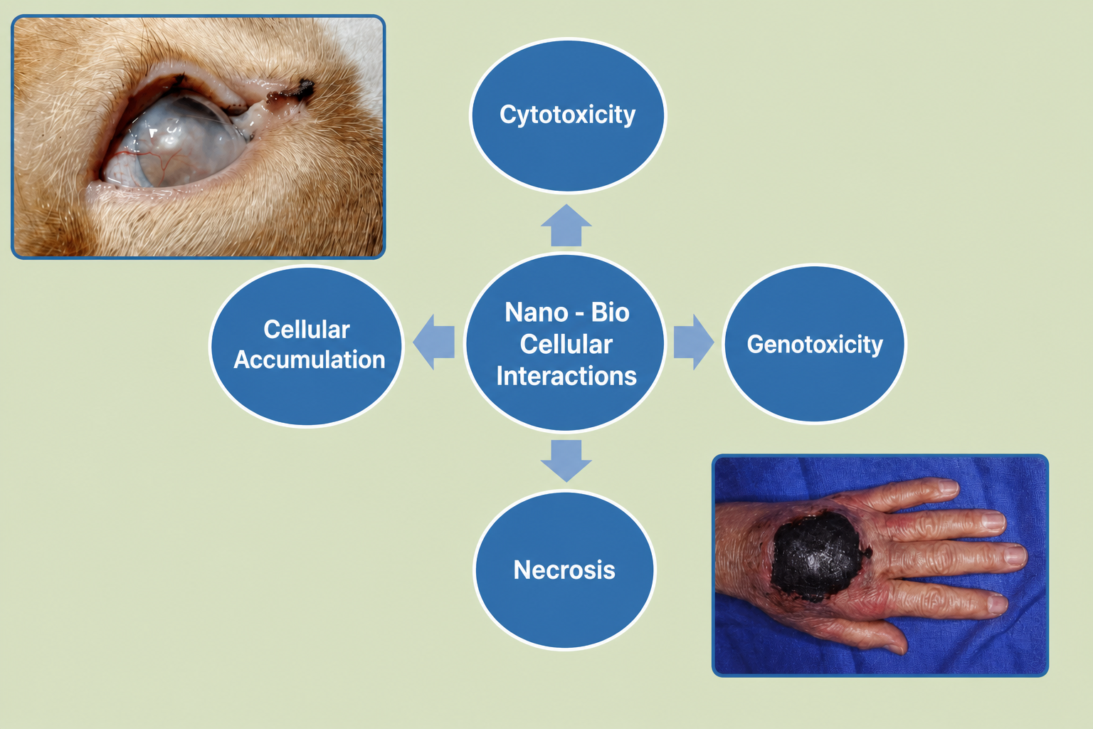
Fig. 24.5 Nano–bio cellular interaction pathways. Nanoparticles entering cells can trigger cytotoxicity, genotoxicity, necrosis, or cellular accumulation, with biological consequences ranging from inflammation to tissue death.
Possible disease associations. Chronic low-level exposure to nanomaterials through inhalation, ingestion, or dermal routes has been tentatively linked to a range of pathological conditions: Alzheimer's and Parkinson's disease (if nanoparticles reach the brain via the olfactory route or blood–brain barrier translocation); lung cancer and asthma (pulmonary deposition); colon cancer (gastrointestinal accumulation); cardiovascular effects including hypertension (circulatory translocation); and dermatitis (skin inflammation from topical products). These associations are still under active epidemiological and toxicological investigation, and causality has not been established for most.
Ingested nanoparticles. Nanoparticles are now found in processed foods as additives — as thickening agents, whitening pigments (TiO₂, E171), taste enhancers, and nutrient carriers — and as incidental contaminants from packaging materials. The titanium content of common confectionery products measured in micrograms of Ti per milligram of food reveals substantial exposures from everyday items including chewing gums, candies, and puddings. The long-term health implications of this chronic low-level ingestion are not yet fully characterised, and regulatory frameworks for nano-food additives lag behind industrial deployment.
6 Working Safely with Nanomaterials
Until the toxicological profile of engineered nanomaterials is more fully understood, the precautionary principle mandates strict exposure controls in research laboratories and manufacturing facilities. The three principal routes of inadvertent exposure are inhalation of airborne nanoparticles, dermal absorption through skin contact, and ingestion of contaminated surfaces or food.
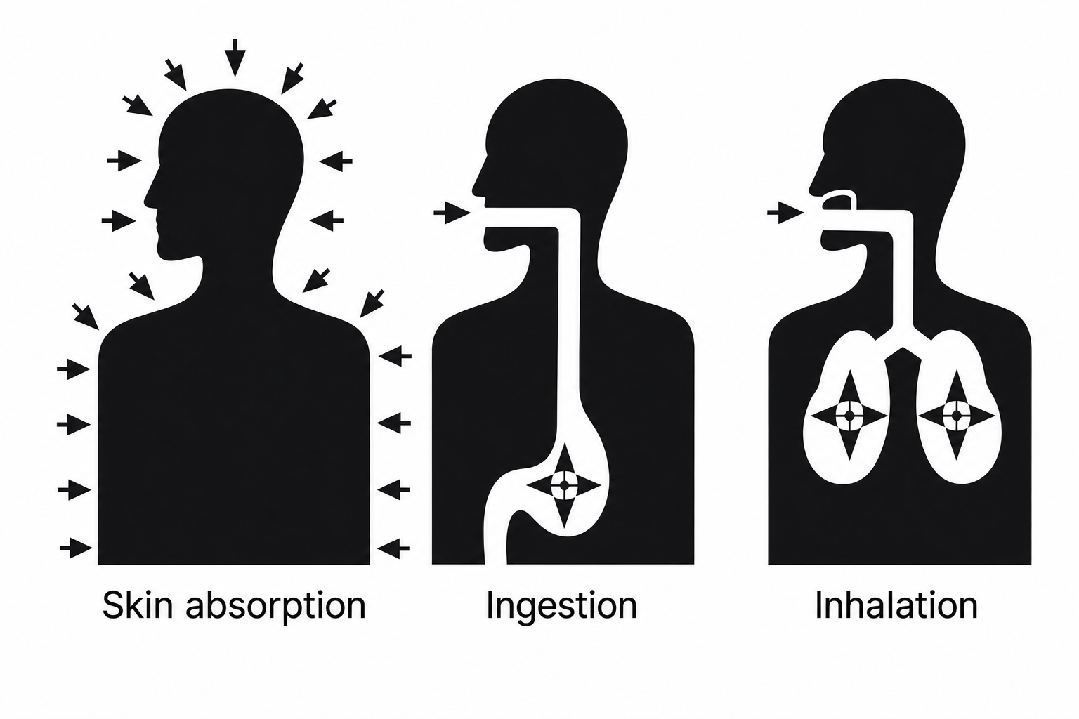
Fig. 24.6 Routes of nanoparticle exposure: skin absorption, ingestion, and inhalation. All three pathways must be controlled in nanomaterial laboratories.
Best-practice nanomaterial safety follows a hierarchy of controls. Engineering controls come first: work inside a biological safety cabinet or fume hood, never on an open bench. Never sweep up dry nanopowder or use compressed air to clean surfaces — both actions aerosolise particles. Use HEPA-filtered vacuum systems and wet-wiping for cleanup. Use sealed containers for transport and label all nanowaste clearly. Wear a properly fitted NIOSH-certified respirator (P100 or N99 minimum), disposable laboratory coat, nitrile gloves, and eye protection. Keep the Material Safety Data Sheet (MSDS/SDS) accessible at all times. Segregate nanowaste and follow institutional disposal protocols.
HEPA — High-Efficiency Particulate Air — filters are the engineering cornerstone of nanoparticle containment. A true HEPA filter captures 99.97% of particles at 0.3 μm (the most penetrating particle size) and performs even better for smaller and larger particles due to the combined effects of diffusion, interception, and inertial impaction. In the nanoparticle range (1–100 nm), diffusion dominates: smaller particles have higher diffusivity and are captured more efficiently than 0.3 μm particles, making HEPA filters highly effective even for the smallest engineered nanoparticles.
The broader question of whether nanotechnology represents a curse or a blessing for human health and the environment cannot yet be answered definitively. The same properties that make nanomaterials transformative in medicine, energy, and electronics — extreme reactivity, size-dependent behaviour, the ability to penetrate biological barriers — are precisely the properties that create risk. The path forward is not prohibition but informed risk management: better fundamental understanding of nano–bio interactions, transparent labelling of nano-enabled products, rapid regulatory adaptation, and continued development of safer-by-design nanomaterials in which toxicologically problematic features are engineered out from the start.
✦ References & Further Reading
- Müller, E. W. & Tsong, T. T. (1969). Field Ion Microscopy: Principles and Applications. Elsevier.
- Miller, M. K. et al. (1996). Atom Probe Field Ion Microscopy. Oxford University Press.
- Oberdörster, G., Oberdörster, E. & Oberdörster, J. (2005). Nanotoxicology: An emerging discipline evolving from studies of ultrafine particles. Environmental Health Perspectives, 113(7), 823–839.
- Nel, A. et al. (2006). Toxic potential of materials at the nanolevel. Science, 311, 622–627.
- Borm, P. J. A. et al. (2006). The potential risks of nanomaterials: A review carried out for ECETOC. Particle and Fibre Toxicology, 3, 11.
Key Takeaways
- FIM uses field-ionised noble gas atoms rather than electrons or photons, achieving resolution at the interatomic scale (~2–5 Å) — sufficient to image individual surface atoms.
- The specimen is a cryogenically cooled (20–100 K) metal needle with a 5–50 nm tip radius; the enormous electric field (~10¹⁰ V m⁻¹) ionises adsorbed gas atoms that project radially onto a fluorescent screen.
- FIM images reveal crystal symmetry, grain boundaries, dislocations, and point defects directly; combining FIM with time-of-flight mass spectrometry creates the 3D atom probe, which reconstructs elemental maps atom by atom.
- The high surface-area-to-volume ratio of nanomaterials means surface reactivity per unit mass is orders of magnitude higher than bulk — the toxicologically relevant dose is surface area, not mass.
- Specific concerns include enhanced photocatalytic activity of nano-TiO₂ in skin products, nanoparticle translocation across biological barriers (lung, gut, brain), and cytotoxicity/genotoxicity/necrosis as cellular interaction modes.
- Safe handling requires engineering controls (biosafety cabinet, fume hood, HEPA filtration), no sweeping or compressed-air cleaning, sealed containers for transport, respirator + disposable coat + gloves, and proper nanowaste disposal.
Scanning Tunnelling Microscopy & Atomic Force Microscopy
Two cornerstone scanning probe techniques — STM and AFM — that image surfaces at atomic and nanometre resolution, their operating principles, scanning modes, and representative applications.
Contents
1 Scanning Probe Microscopy — Overview
Scanning probe microscopy (SPM) is a family of imaging techniques in which a sharp physical probe is raster-scanned across a surface and a local physical interaction between tip and sample is used to build up a point-by-point image. Unlike electron microscopies, SPM methods do not require a vacuum or a beam of particles — they work in air, liquid, or vacuum — and they interact directly with the atomic and molecular structure of the surface rather than forming a projected shadow image. The two most important members of the family are the scanning tunnelling microscope (STM), which senses quantum-mechanical tunnelling current, and the atomic force microscope (AFM), which senses interatomic forces.
2 Scanning Tunnelling Microscopy — Principle
The STM was invented by Gerd Binnig and Heinrich Rohrer at IBM Zürich in 1981, earning them the Nobel Prize in Physics in 1986. It exploits a quantum-mechanical effect that classical physics cannot account for: when two conductors are brought within about 1 nm of each other without touching, electrons can tunnel quantum-mechanically across the vacuum gap and produce a measurable electric current even though no classical path exists. This tunnelling current is extraordinarily sensitive to the gap width, falling by approximately one order of magnitude for every 0.1 nm increase in separation.
The instrument consists of a very sharp metallic tip — ideally terminating in a single atom — that is connected to a piezoelectric scanner capable of moving the tip in three dimensions with sub-ångström precision. A small bias voltage of a few millivolts to a few volts is applied between tip and sample. When the tip is brought to within roughly 0.3–1 nm of a conducting surface, a tunnelling current of order 0.1–10 nA flows. This current is amplified and fed into a feedback control loop that adjusts the vertical position of the tip. By raster-scanning the tip laterally across the surface while the feedback loop maintains either a constant current or a constant height, the STM records the three-dimensional topography of the surface at atomic resolution.
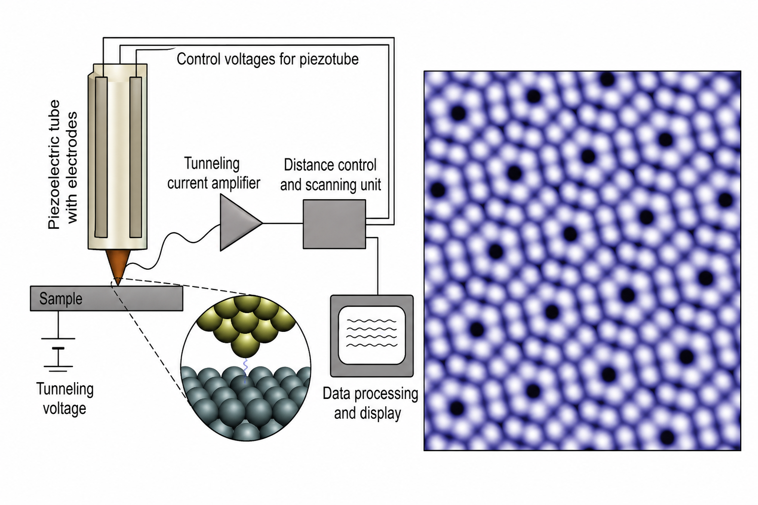
Fig. 25.1 Left: schematic of STM operation. The piezoelectric tube positions the tip, the tunnelling current is amplified and fed to a distance control unit that adjusts tip height. Right: atomic-resolution STM image of the Si(111) 7×7 surface reconstruction, showing individual silicon adatoms arranged in the characteristic hexagonal unit cell.
In a well-isolated STM system free from external mechanical vibration, the instrument routinely achieves sub-ångström vertical resolution (sensitivity to height changes of ~0.01 Å) and atomic lateral resolution (~1–2 Å). This makes STM the highest-resolution imaging method for electrically conductive surfaces. The limitation is that the sample and tip must both be electrically conducting — insulators cannot sustain a tunnelling current.
3 STM Scanning Modes
The STM probe can be operated in two fundamentally different scanning modes, each suited to different surface types and experimental goals.
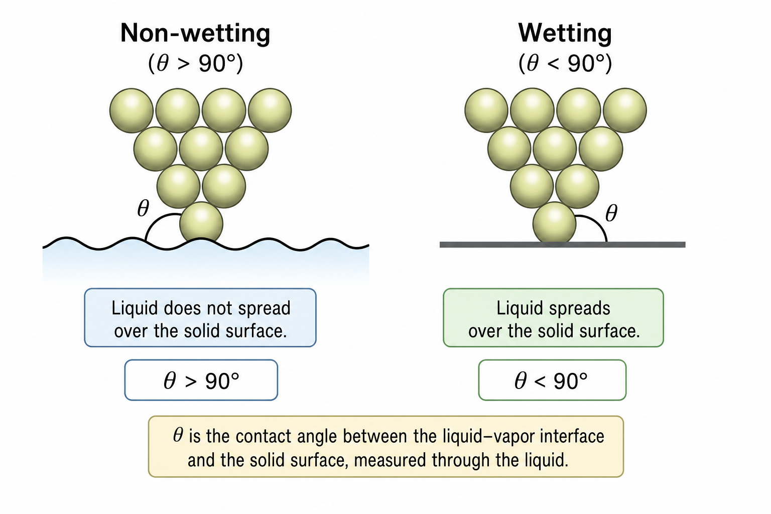
Fig. 25.2 STM scanning modes: (a) constant-current mode — the tip follows the surface contour via feedback, tracing a wavy path proportional to topography; (b) constant-height mode — the tip is held at a fixed height and variations in tunnelling current encode the surface structure.
Constant-height mode. The tip is held at a fixed vertical position while scanning laterally, and variations in the tunnelling current at each point encode information about the local surface structure. Because the tunnelling current is extremely sensitive to small height modulations at the atomic scale, this mode is excellent for imaging atomically smooth surfaces at high speed. It does not require the feedback loop to respond rapidly, so scan speeds can be faster — but if the surface has significant topographic variation, the tip risks crashing into step edges or large features.
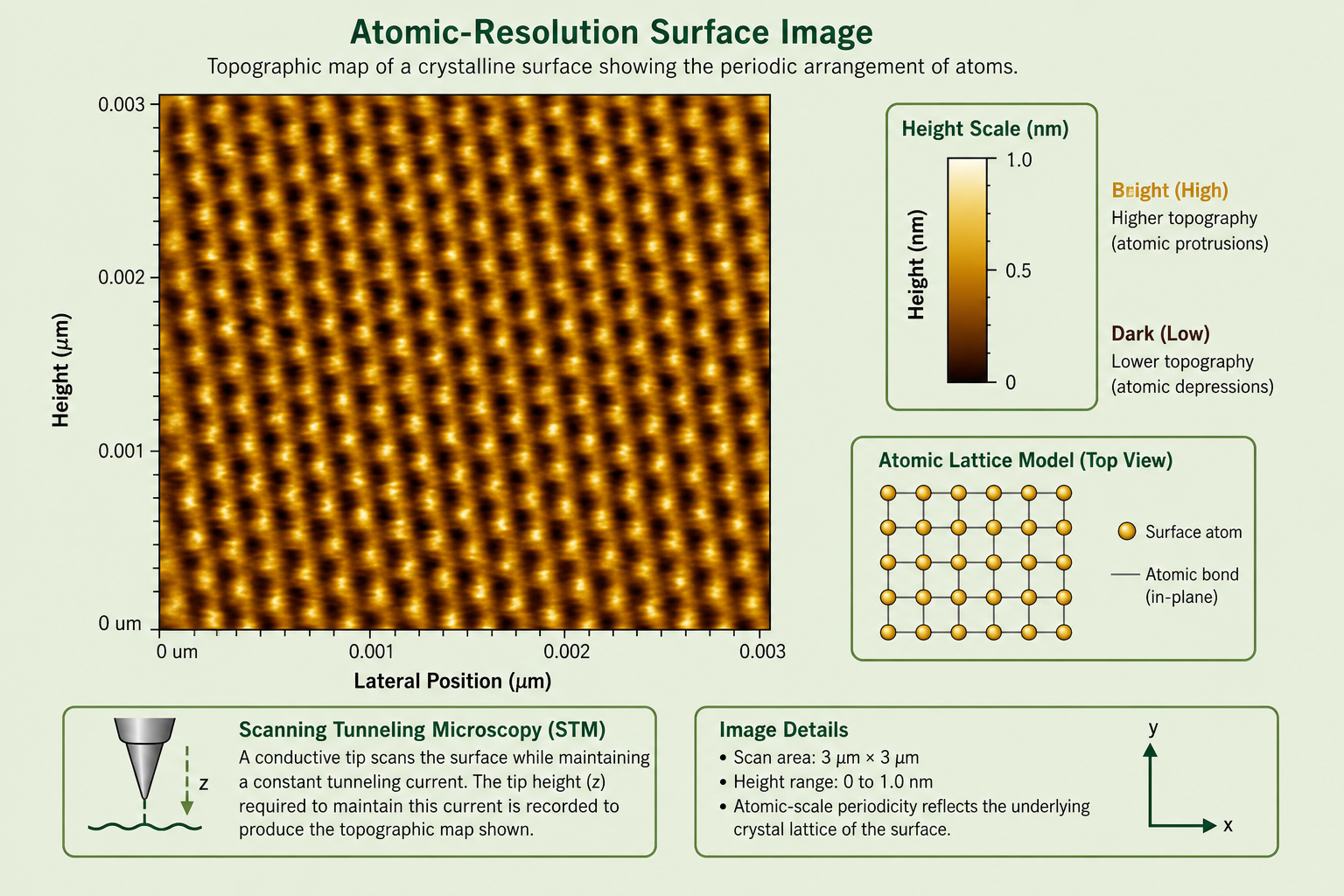
Fig. 25.3 STM image of HOPG (highly ordered pyrolytic graphite) in constant-height mode. The bright spots correspond to carbon atoms at every other lattice site of the graphene honeycomb (the electronic asymmetry between A and B sites of graphite makes only one sublattice visible). Scan area 3×3 nm.
Constant-current mode. An electronic feedback loop continuously adjusts the tip height to keep the tunnelling current constant as the tip scans laterally. The vertical movement of the scanner required to maintain constant current is recorded and directly yields the surface topography. This mode is suitable for surfaces with significant roughness or step structure, as the tip actively follows the contour and the risk of crashing is minimised. It measures topography with high accuracy but is inherently slower than constant-height mode because the feedback loop must respond to each height change as the tip moves.
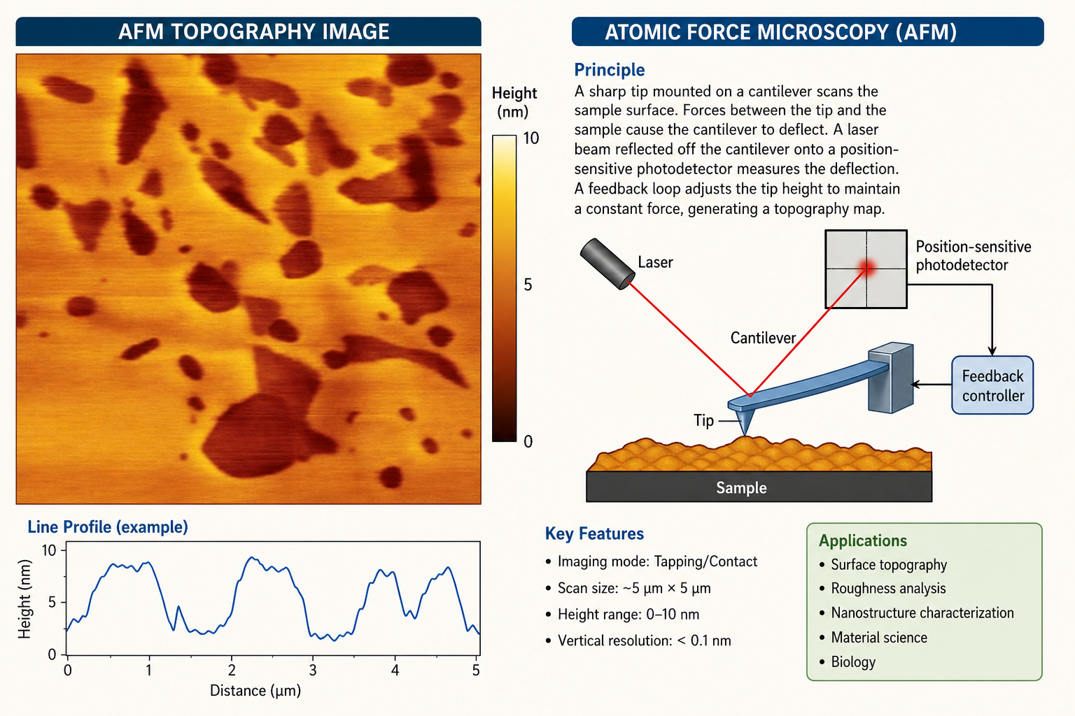
Fig. 25.4 STM topography of HOPG in large-scale constant-current mode (−100 mV, 2.0 nA, 315×336 nm² scan). The dark recessed regions represent steps or folded graphene layers at the surface; the green arrow marks an overlapping dark pattern characteristic of twisted graphene domains. Constant-current mode faithfully maps the full topographic range of this rough area.
Use constant-height mode for atomically flat surfaces where high scan speed and sensitivity to fine electronic modulations are needed. Use constant-current mode for surfaces with significant topographic variation — step edges, islands, nanoparticles — where maintaining a safe tip-sample distance is paramount and high topographic accuracy is required.
4 Atomic Force Microscopy — Principle
The atomic force microscope was developed by Binnig, Quate, and Gerber in 1986 as a direct extension of the STM concept to non-conducting materials. The critical distinction between STM and AFM is the interaction sensed: STM measures quantum-mechanical tunnelling current (requiring both tip and sample to be conductive), while AFM measures the interatomic force between the tip and the sample surface. Because atomic forces act between any two atoms regardless of their electrical character, AFM can image insulators, semiconductors, polymers, biological membranes, living cells, and virtually any material — a huge practical advantage over STM.
In AFM, the sharp tip — typically silicon or silicon nitride with a radius of curvature as small as 20 nm — is mounted at the free end of a microfabricated cantilever beam. When the tip is brought close to or into contact with the surface, short-range repulsive forces (contact regime), long-range van der Waals and electrostatic attractive forces (non-contact regime), or a combination of both act on the tip and deflect the cantilever. The physical properties of the cantilever — its spring constant, resonant frequency, length, width, and thickness — are carefully engineered because the detection systems used in AFM depend on the amplitude, phase, or frequency of vibration of the cantilever.
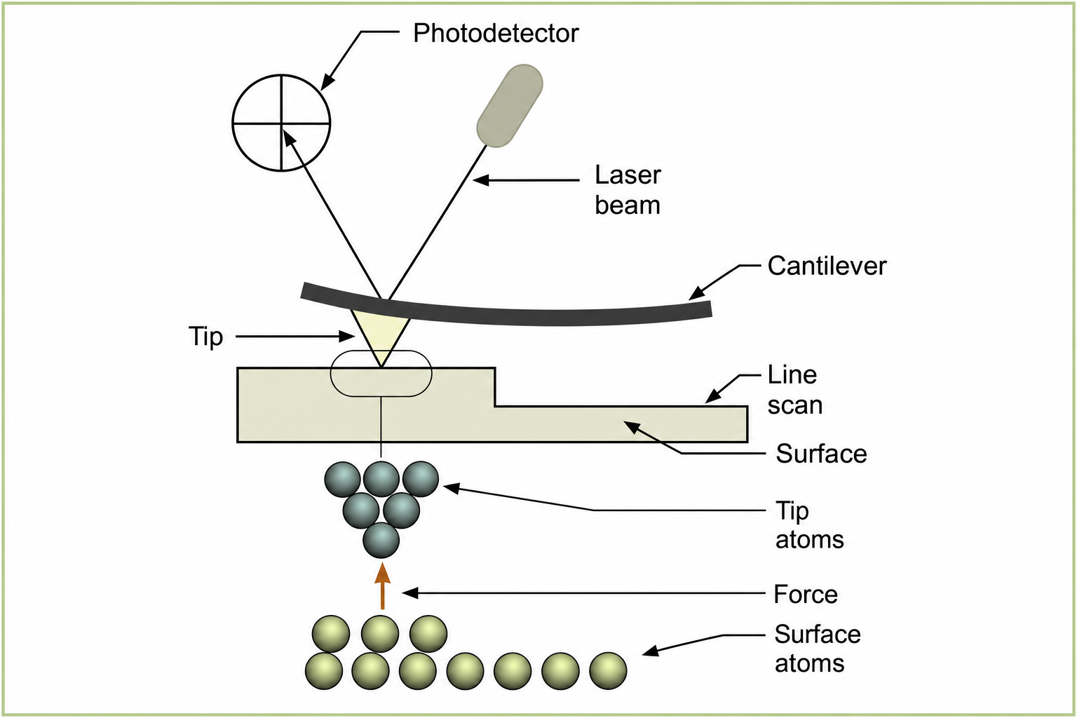
Fig. 25.5 AFM schematic. A laser beam reflects off the back of the cantilever onto a position-sensitive split photodetector. Any deflection of the cantilever caused by tip–surface forces shifts the reflected spot on the detector, providing an electrical signal proportional to force. The cantilever's deflection is a function of its elastic modulus and geometry (Beam: Deflection = f(Elastic modulus, dimension)).
The deflection of the cantilever is detected optically: a laser beam is focused on the reflective back surface of the cantilever and the reflected beam falls on a position-sensitive photodetector (typically a quadrant photodiode). Sub-ångström deflections of the cantilever shift the laser spot on the detector by a measurable amount. This optical lever detection scheme amplifies small cantilever displacements by the ratio of the detector-to-cantilever distance to the cantilever length, providing extremely sensitive force detection in the range of piconewtons.
5 AFM Operating Modes
AFM can be operated in three primary modes, each exploiting a different force regime and offering different compromises between resolution, sample damage, and imaging speed.
Contact mode. The tip is in direct physical contact with the sample surface throughout scanning. Short-range repulsive forces dominate the interaction, and the applied force between tip and sample is held constant by the feedback loop as the cantilever deflection is maintained at a setpoint. Surface topography is encoded in the vertical piezo movement required to maintain constant deflection. Contact mode provides high lateral resolution but can damage soft samples (biological membranes, polymers, loosely adsorbed layers) through the lateral shear forces generated as the tip drags across the surface.
Non-contact mode. The cantilever is vibrated at or near its resonant frequency at an amplitude of a few nanometres, and the tip is held at a distance of several nanometres above the surface — far enough that it does not physically touch. The long-range attractive van der Waals forces between tip and surface alter the effective spring constant of the cantilever, shifting its resonant frequency. By monitoring changes in the amplitude, phase, or natural frequency of the cantilever oscillation, the feedback system maps surface topography without any physical contact. This is ideal for imaging delicate samples but is sensitive to contamination layers (adsorbed water) and tends to give lower resolution than contact or tapping modes under ambient conditions.
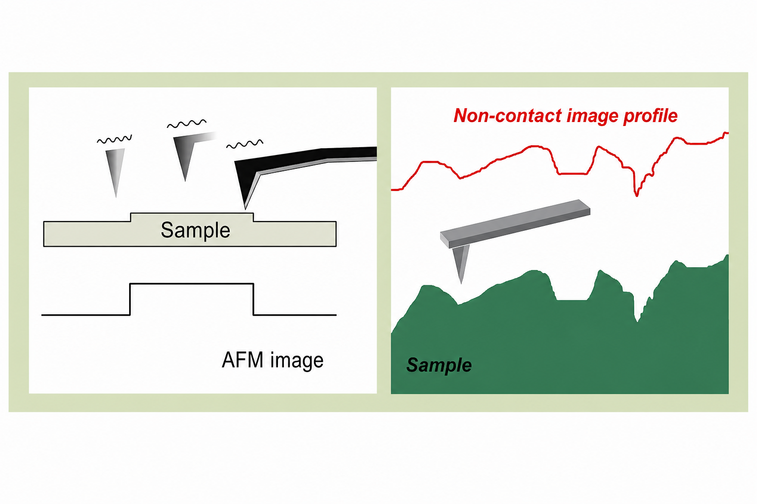
Fig. 25.6 AFM non-contact mode. Left: the vibrating cantilever is held above a stepped sample; the resulting AFM image profile faithfully reproduces the step topography without contact. Right: the non-contact image profile (red) tracks the true surface (green) as the cantilever hovers above without touching — note the slight overestimation of feature heights due to force-averaging in the attractive regime.
Tapping mode (intermittent contact). Tapping mode is a compromise between contact and non-contact AFM. The cantilever is oscillated at its resonant frequency with a large free amplitude (typically 20–100 nm), and the tip briefly taps the surface at the bottom of each oscillation cycle. The feedback loop maintains a constant oscillation amplitude (a setpoint) by adjusting the tip–sample distance. Because the tip only touches the surface intermittently and the lateral sliding motion of contact mode is eliminated, tapping mode dramatically reduces shear forces and is much less likely to damage soft samples. The amplitude of oscillation determines the topographic contrast, and phase imaging (recording phase shifts between the drive oscillation and the cantilever response) provides additional contrast related to local viscoelastic properties, adhesion, and composition.
6 AFM Imaging Examples — Biological Applications
The ability of AFM to image in liquid environments at room temperature under near-physiological conditions makes it exceptionally valuable for studying biological nanomaterials. Unlike electron microscopy, which requires vacuum and typically demands sample fixation or staining, AFM can image living cells, protein assemblies, DNA, lipid membranes, and drug nanocarriers in their native hydrated state.
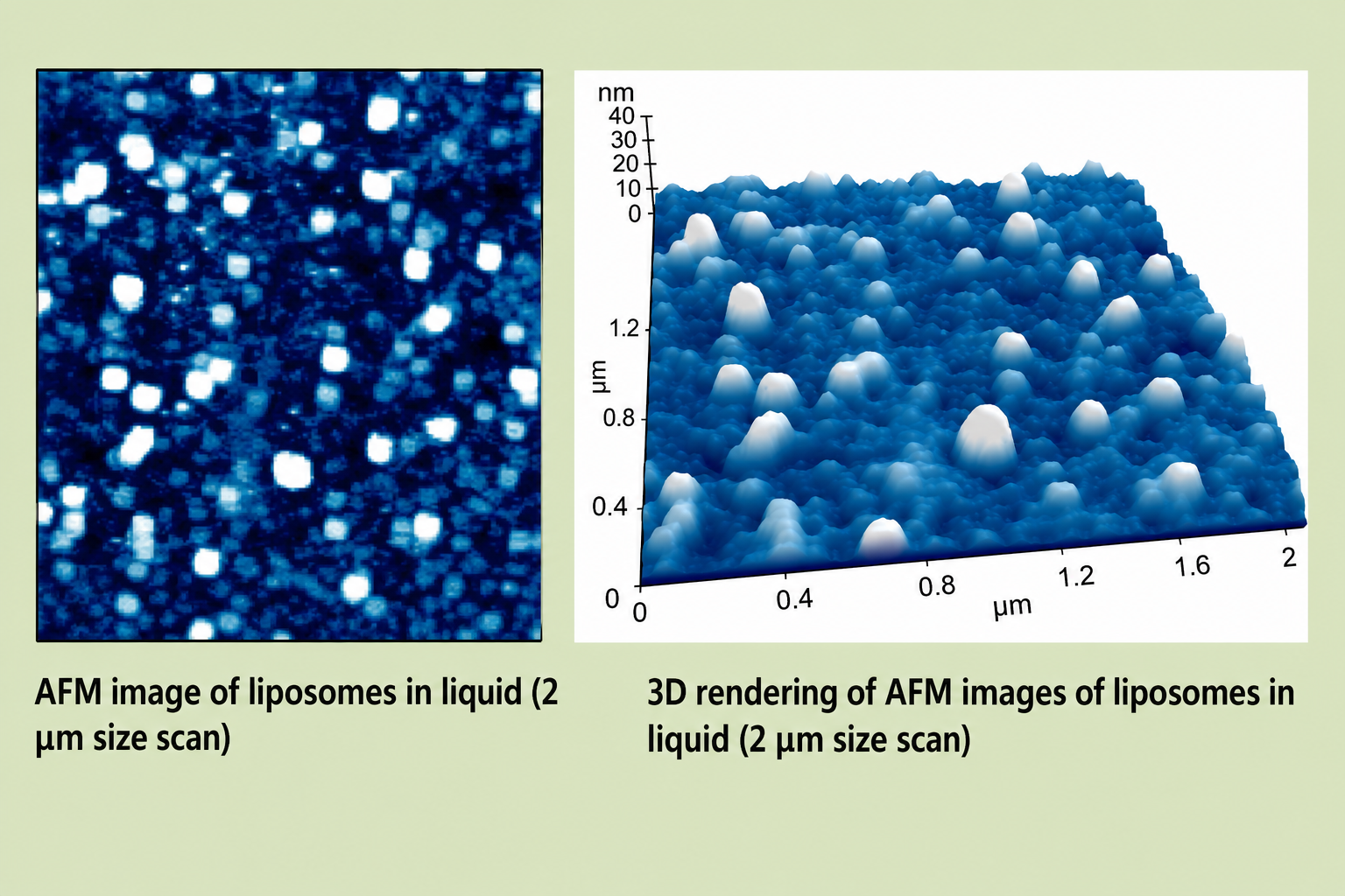
Fig. 25.7 AFM imaging of liposomes in liquid (2 μm scan area). Left: conventional 2D height image — bright spots are individual liposomes adsorbed on a flat substrate. Right: 3D rendered height map of the same data, revealing the dome-shaped morphology of each vesicle (heights up to ~40 nm) and the distribution of particle sizes.
STM requires the sample to be electrically conducting and measures quantum-mechanical tunnelling current; it achieves true atomic resolution on clean metal and semiconductor surfaces. AFM measures interatomic forces and can image any material — conducting, semiconducting, or insulating — including biological samples in liquid. AFM resolution is typically 1–5 nm laterally in ambient conditions (though atomic resolution is achievable in UHV), and it provides direct force measurements in addition to topography. In practice, STM is preferred for atomic-resolution studies of clean surfaces while AFM is indispensable for soft matter, insulators, and biological systems.
✦ References & Further Reading
- Binnig, G., Rohrer, H., Gerber, Ch. & Weibel, E. (1982). Surface studies by scanning tunneling microscopy. Physical Review Letters, 49, 57.
- Binnig, G., Quate, C. F. & Gerber, Ch. (1986). Atomic force microscope. Physical Review Letters, 56, 930.
- Stroscio, J. A. & Kaiser, W. J. (Eds.) (1993). Scanning Tunneling Microscopy. Academic Press.
- Eaton, P. & West, P. (2010). Atomic Force Microscopy. Oxford University Press.
- Jalili, N. & Laxminarayana, K. (2004). A review of atomic force microscopy imaging systems. Mechatronics, 14, 907–945.
Key Takeaways
- STM uses quantum-mechanical tunnelling current between a sharp metal tip and a conductive surface; current decays by ~10× per 0.1 nm gap change, giving sub-ångström vertical resolution and atomic lateral resolution.
- STM is restricted to electrically conductive surfaces; a piezoelectric scanner with sub-ångström precision moves the tip in all three dimensions.
- Constant-height mode holds the tip at fixed z and maps current variations — fast, best for flat surfaces. Constant-current mode uses feedback to maintain constant current and maps the tip's z-movement — slower, topographically accurate, safe for rough surfaces.
- AFM measures interatomic forces via deflection of a microfabricated cantilever detected by an optical lever (laser + position-sensitive photodetector); it can image any material, including insulators and biological specimens.
- Three AFM modes: contact (tip in continuous contact, shear forces, risk of sample damage), non-contact (cantilever vibrated above surface, frequency/amplitude shift, no contact, good for delicate samples), and tapping (intermittent contact at resonance, reduced shear, most versatile).
- AFM in liquid enables imaging of biological nanostructures — liposomes, proteins, DNA, membranes — in near-native conditions, an application inaccessible to STM or electron microscopy without special preparation.
Near-Field Scanning Optical Microscopy
Optical characterisation beyond the diffraction limit — how bringing a nanoscale probe within 10 nm of a surface unlocks spatial resolution that conventional far-field optics can never achieve.
Contents
- Characterisation at the Nanoscale — an Overview
- Why Optical Characterisation Matters
- The Diffraction Limit and the Near-Field Concept
- Instrument Design and Probe Construction
- Near-Field vs Far-Field Resolution
- Operating Modes
- Example Image: NSOM of Clean Glass
- Applications of NSOM
- References & Further Reading
1 Characterisation at the Nanoscale — an Overview
Every nanomaterial study begins with a question of what the material actually looks like and what it is made of. Because nanoscale features cannot be seen or probed with the naked eye or with ordinary optical equipment, a family of specialised characterisation techniques has been developed, each suited to a particular range of length scales and each returning a different type of information.
The chart below summarises the principal techniques and what they deliver. Near-field and confocal light microscopy report on size, shape, topography, and — in the confocal variant — full 3D image reconstruction. Transmission Electron Microscopy (TEM) adds crystallographic information inferred from diffraction patterns in addition to size and composition. Scanning Electron Microscopy (SEM) extends the picture to include microstructure, topography, and grain orientation across a wide field of view. X-ray diffraction measures size, crystal structure, and lattice strain. Atomic Force Microscopy (AFM) maps surface topography and mechanical properties with sub-nanometre vertical resolution. Spectroscopic methods round out the toolkit by providing chemical composition and bonding state through techniques such as XPS, EDS, and Raman.
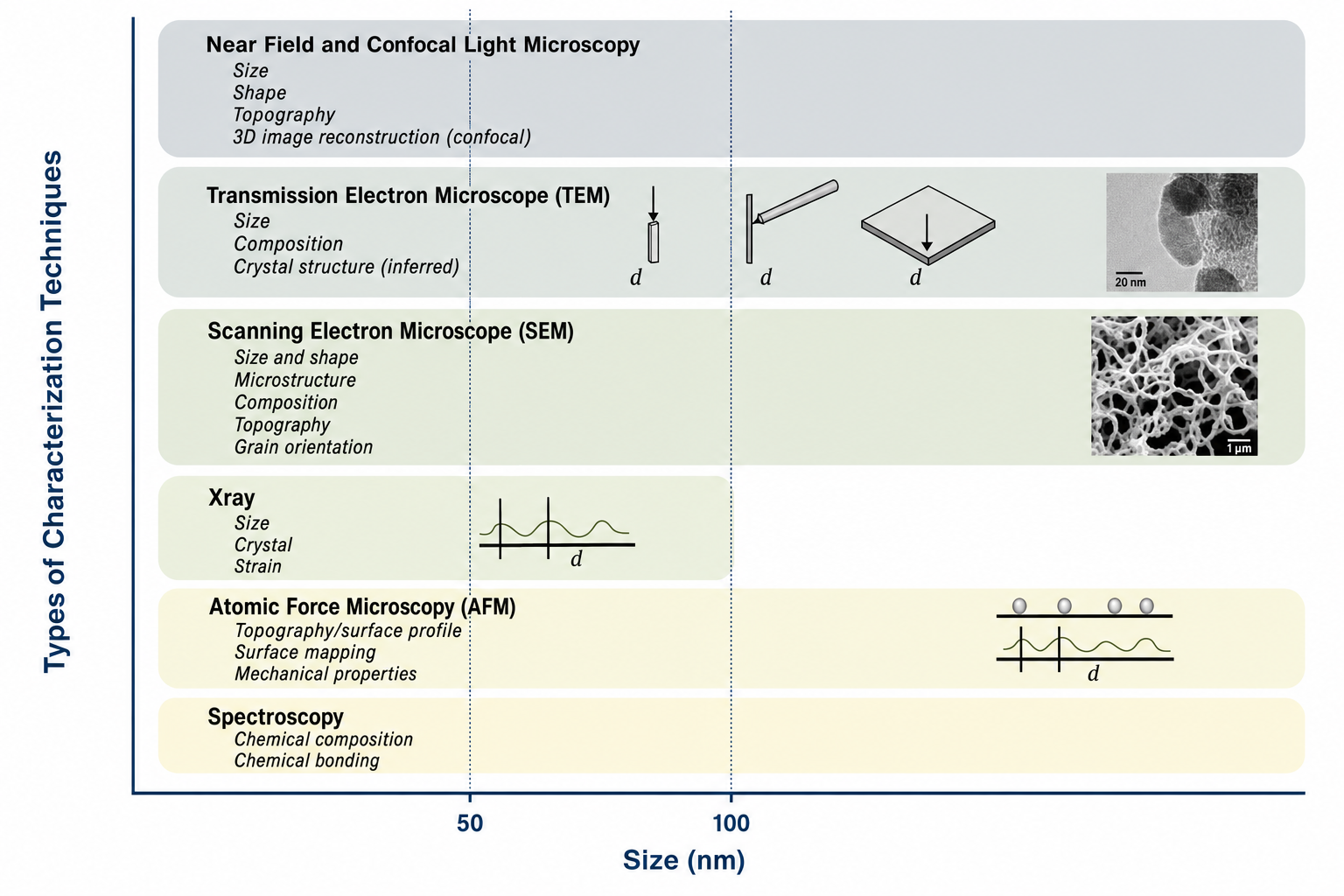
Fig. 26.1 Overview of nanoscale characterisation techniques and the classes of information each provides.
The choice of technique for any given nanomaterial is governed by two criteria: the resolution of information required, and the type of information sought. Imaging involves microscopy and analysis involves spectroscopy, with excitation delivered by light, ions, electrons, or scanning probes depending on the instrument.
2 Why Optical Characterisation Matters
Light is not merely a tool of convenience — it is deeply embedded in both the scientific investigation of nanomaterials and in the natural systems that nanomaterials are often designed to interact with. Photosynthesis, the most important energy-conversion process on Earth, is driven by light. Scientific research fields rely on optical phenomena including absorption, fluorescence, photoinduced electron transfer, light-emitting devices, and photovoltaic cells. Characterising how a nanomaterial interacts with light is therefore central to understanding its function in real applications.
Near-field scanning optical microscopy, or NSOM, belongs to the category of light microscopes. It was developed specifically to overcome the fundamental resolution ceiling that limits all conventional optical instruments — a ceiling set by the wavelength of light itself.
3 The Diffraction Limit and the Near-Field Concept
In any conventional far-field optical system, two points separated by less than approximately λ/2 cannot be resolved as distinct objects. For visible light with a wavelength of roughly 600 nm, this sets a practical resolution floor of about 300 nm. No amount of engineering of lenses, apertures, or detectors can circumvent this limit within a far-field geometry — it is a consequence of wave diffraction, not of instrument imperfection.
The near-field concept sidesteps diffraction entirely. If a nanometre-scale aperture is brought to within a distance much smaller than the aperture diameter from the surface being examined, the light that emerges from that aperture illuminates only a tiny, well-defined spot before it has had the opportunity to diffract and spread. The illuminated area is governed not by the wavelength of light but by the physical dimensions of the aperture. This is the regime of the near field — where the evanescent components of the electromagnetic field, which decay exponentially with distance and carry information at length scales far below λ, can be sampled before they are lost.
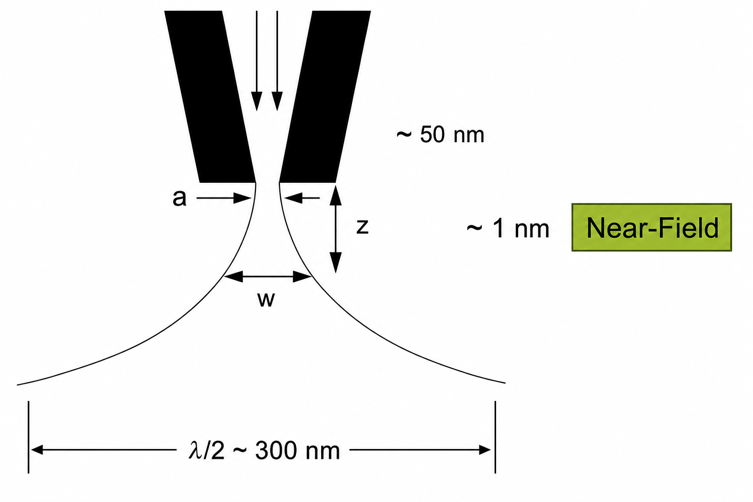
Fig. 26.2 Geometry of near-field illumination. Resolution is set by aperture width a and probe-to-sample distance z, not by the wavelength. The near-field zone extends only ~1 nm beyond the aperture; high spatial resolution therefore demands that the probe be kept extremely close to the surface.
There is, however, a fundamental trade-off. Making the aperture smaller improves spatial resolution but also reduces light throughput — a very small aperture passes very little light, lowering signal intensity and ultimately setting a practical floor on the aperture size that can be used. Typical NSOM operation balances these competing demands at aperture diameters of 50–100 nm, yielding spatial resolution of around 50 nm — roughly six times better than the diffraction limit.
4 Instrument Design and Probe Construction
The NSOM instrument consists of two principal components: the optical head, which delivers and collects light through a nanoscale probe; and a feedback control system, which maintains the probe at a fixed, very small distance above the sample surface while it rasters across it.
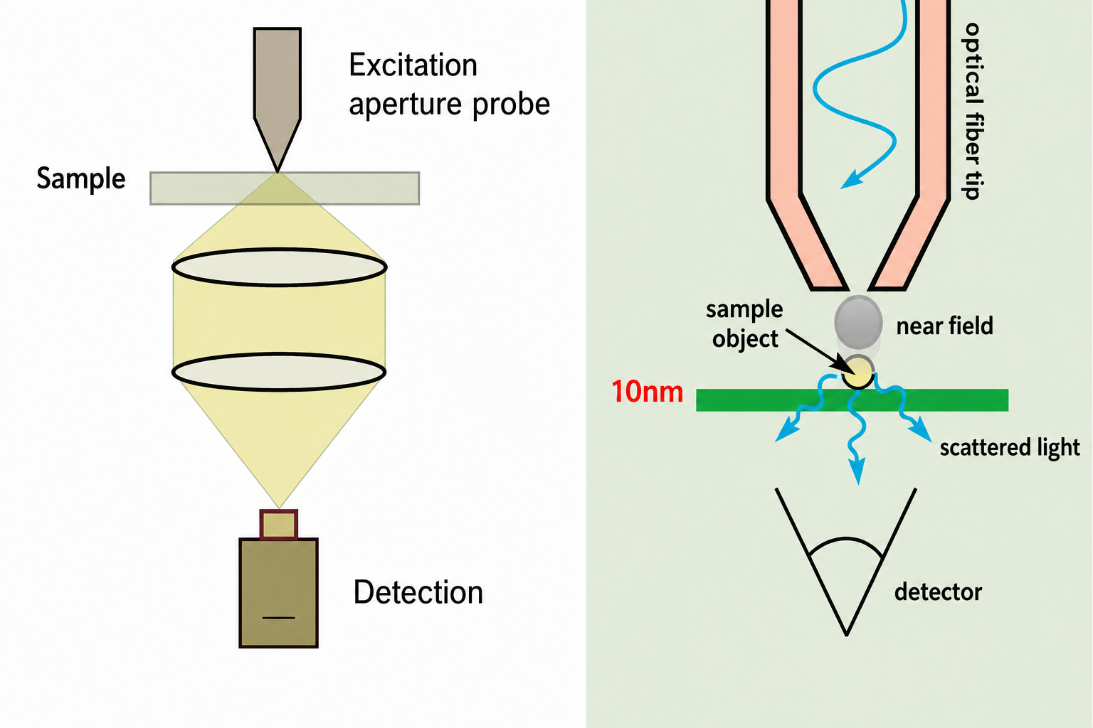
Fig. 26.3 NSOM instrument layout. Left: the excitation aperture probe illuminates the sample; transmitted light is collected below. Right: the optical fiber tip at 10 nm from the sample object, showing the near-field interaction zone and scattered-light collection.
The probe is an optical fibre that has been drawn to a sharp taper and coated with an opaque metal (typically aluminium) on all sides except a tiny opening at the very apex — the aperture through which light enters or exits. The core and cladding of the fibre guide light to the tip; the metallic coating prevents light from leaking through the sides. The aperture itself, at the apex, has a diameter of 50–100 nm.
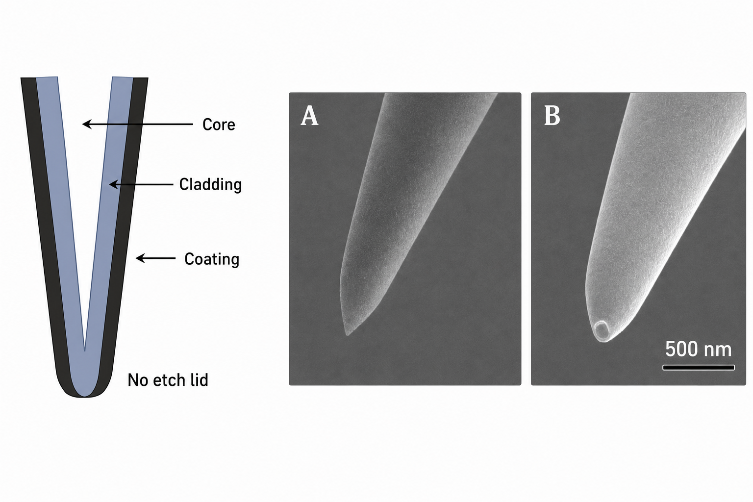
Fig. 26.4 NSOM fiber tip structure. Left: cross-section schematic showing core, cladding, and metallic coating. A and B: SEM images of fabricated tips; the scale bar in B is 500 nm.
For high spatial resolution, the probe must be kept extremely close to the sample — typically 5–10 nm above the surface, well within the near-field zone. Distance control is usually achieved by monitoring a shear-force feedback signal (an oscillating probe detects damping as it approaches the surface), or by using the fibre tip as a contact-mode AFM cantilever simultaneously.
5 Near-Field vs Far-Field Resolution
The comparison between NSOM and a conventional far-field lens illustrates the resolution advantage starkly. When a far-field objective collects light that has passed through the sample, the smallest feature it can resolve is determined by the Abbe diffraction limit: approximately λ/2 ~ 300 nm for visible light. When an NSOM tip is used in its place, the illuminated spot at the sample is defined by the aperture, giving a resolution of ~50 nm — a six-fold improvement. The near-field regime itself, where the evanescent field is most intense, extends only ~1 nm beyond the aperture, making probe proximity the critical engineering challenge.
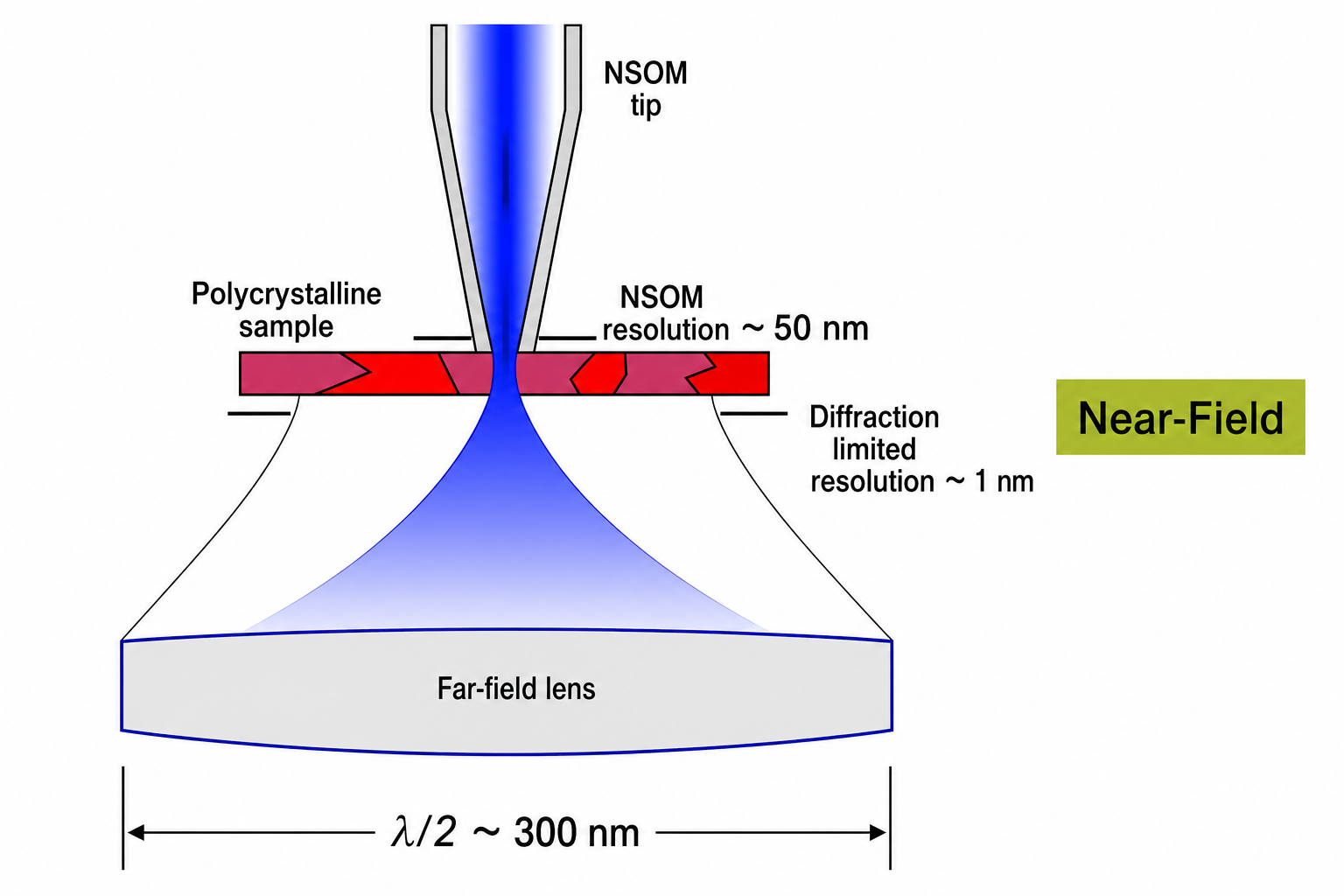
Fig. 26.5 NSOM resolution versus diffraction-limited far-field resolution. The NSOM tip delivers ~50 nm lateral resolution at the sample surface, compared with the ~300 nm diffraction limit of a far-field lens.
6 Operating Modes
NSOM can be configured in several geometries depending on whether the tip is used to deliver light to the sample, collect light from it, or both. The five principal modes are:
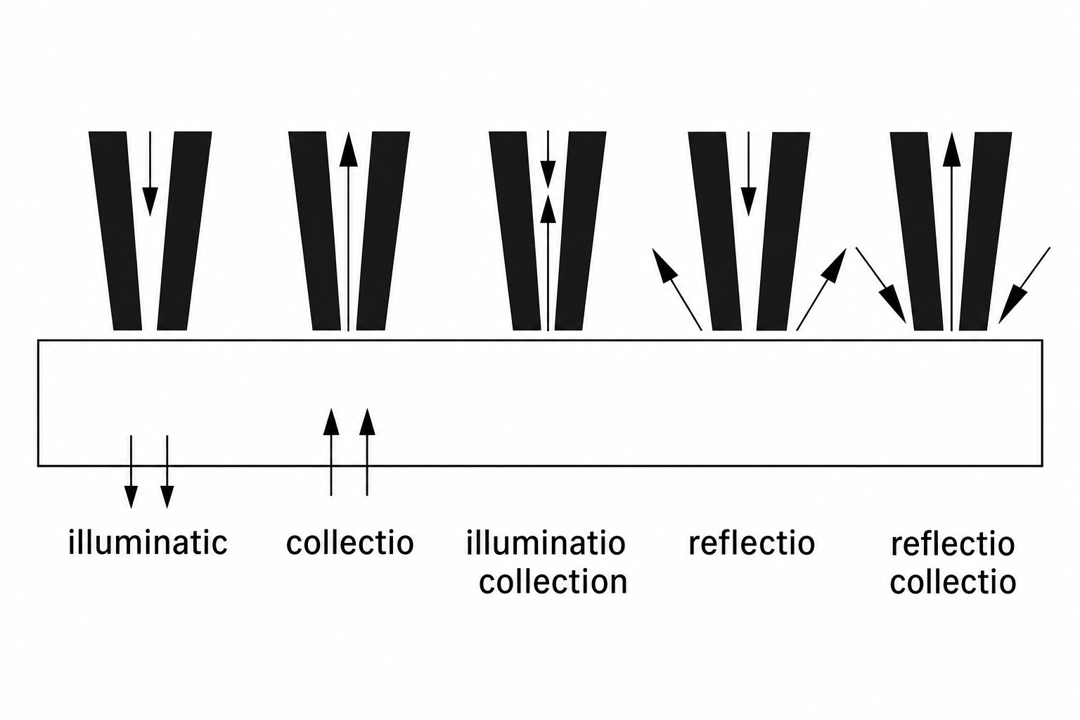
Fig. 26.6 The five NSOM operating modes, from left to right: illumination, collection, illumination-collection, reflection, and reflection-collection.
Illumination mode — Light is launched down the fibre and emerges from the tip aperture to illuminate the sample locally; the transmitted or fluorescent signal is collected by a far-field objective beneath the sample. This is the simplest mode to implement and interpret, and it yields the strongest signal. It requires a transparent sample, which limits its use for opaque materials such as silicon or many biological specimens.
Collection mode — The sample is illuminated from below by a conventional far-field source; the tip collects the near-field signal from a nanoscale region of the surface. Signal levels are lower than in illumination mode.
Illumination-collection mode — The tip both illuminates and collects at the same aperture, operating in reflection. This provides a useful complement to the transmission modes but carries a larger background signal, which makes it challenging for spectroscopic applications.
Reflection and reflection-collection modes — These allow opaque samples to be studied. Signal levels are lower and the result is more sensitive to tip geometry, but they extend NSOM to the full range of materials including metals, semiconductors, and thick biological samples.
7 Example Image: NSOM of Clean Glass
A striking demonstration of NSOM capability is the surface topography of a clean glass substrate — a material that appears perfectly featureless to conventional optical microscopy. The NSOM image below reveals genuine nanometre-scale roughness: a corrugated landscape of bumps and troughs with a peak-to-valley height variation of 1.48 nm over a 6 × 6 µm scan area. This level of detail is entirely invisible to a diffraction-limited instrument.
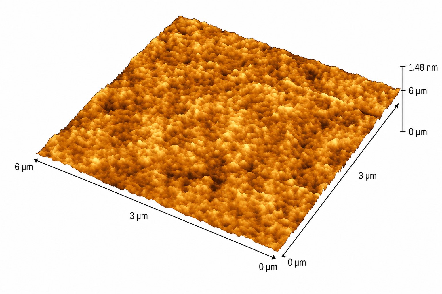
Fig. 26.7 NSOM topography of a clean glass surface. The 6 × 6 µm scan reveals surface roughness with a total height range of just 1.48 nm — detail that is completely unresolvable by diffraction-limited optics.
8 Applications of NSOM
The ability to perform optical characterisation at length scales far below the diffraction limit opens NSOM to a wide range of research applications.
Ultra-high-resolution optical imaging is the primary application. NSOM can map optical contrast — refractive index variation, absorption, scattering — at 50 nm resolution across surfaces of semiconductors, polymers, biological membranes, and photonic structures. Features such as grain boundaries, nanoscale phase domains, and single fluorescent molecules have all been imaged in this way.
Near-field spectroscopy is possible when the aperture is small enough to excite individual nanoscale objects. Fluorescence spectra, Raman spectra, and absorption spectra can in principle be collected from single nanoparticles, quantum dots, or even individual molecules, providing chemical and electronic information at spatial resolutions previously accessible only to electron-beam techniques.
Surface modification using the NSOM tip — both optical (photochemical patterning) and mechanical — makes NSOM a potential nanofabrication tool. The tip can locally expose photoresist, induce chemical reactions, or deliver energy to specific nanoscale regions of a surface. Biological applications include the controlled modification of cell membranes and the patterning of biomolecular arrays.
✦ References & Further Reading
- Betzig, E. & Trautman, J.K. (1992). Near-field optics: microscopy, spectroscopy, and surface modification beyond the diffraction limit. Science, 257, 189–195.
- Pohl, D.W., Denk, W. & Lanz, M. (1984). Optical stethoscopy: image recording with resolution λ/20. Applied Physics Letters, 44, 651–653.
- Novotny, L. & Hecht, B. (2012). Principles of Nano-Optics (2nd ed.). Cambridge University Press.
- Hecht, B., Sick, B., Wild, U.P., Deckert, V., Zenobi, R., Martin, O.J.F. & Pohl, D.W. (2000). Scanning near-field optical microscopy with aperture probes: fundamentals and applications. Journal of Chemical Physics, 112, 7761–7774.
Key Takeaways
- Nanoscale characterisation uses light, electrons, ions, and scanning probes, each returning different structural or chemical information.
- Conventional optics is bounded by the diffraction limit (~λ/2 ≈ 300 nm for visible light); NSOM bypasses this by sampling the evanescent near field at a probe-to-sample distance below the aperture diameter.
- NSOM resolution (~50 nm) is governed by aperture size, not wavelength; smaller apertures improve resolution but reduce signal — a fundamental trade-off.
- The probe is a tapered, metal-coated optical fibre with a nanoscale aperture; maintaining a ~10 nm tip-to-sample gap is the core engineering challenge.
- Five operating modes (illumination, collection, illumination-collection, reflection, reflection-collection) extend NSOM to both transparent and opaque samples.
- Applications span ultra-high-resolution imaging, single-molecule spectroscopy, and localised surface modification in photonic and biological systems.
Chemical Characterisation: EDS, AES & EELS
How electron beams interrogate the chemical identity of nanomaterials — from characteristic X-rays and Auger transitions to inelastic energy losses and the three-region EELS spectrum.
Contents
- Chemical Characterisation by Electron Spectroscopy
- EDS: Energy Dispersive Spectroscopy
- EDS: Resolution, Electron Guns, and STEM
- TEM: Resolution and Accelerating Voltage
- Auger Electron Spectroscopy (AES)
- AES: Properties, Advantages, and Limitations
- AES: Experimental Example
- Electron Energy Loss Spectroscopy (EELS)
- The EELS Spectrum: Three Regions
- Core-Loss Edges: Absorption Edges and Fine Structure
- Absorption Edges and Specimen Thickness Effects
- Comparing EDS, AES, and EELS
- References & Further Reading
1 Chemical Characterisation by Electron Spectroscopy
Structural characterisation tells us about size, shape, and crystal structure. Chemical characterisation answers a different question: what elements are present and in what concentrations? For nanomaterials this is not trivial — a particle only a few nanometres across contains perhaps a few hundred atoms, and its surface chemistry can differ dramatically from its interior. The electron beam provides a remarkably versatile probe because electrons interact with matter through multiple distinct mechanisms, each generating a characteristic signal that carries compositional information.
Three techniques based on electron spectroscopy are the workhorses of nanomaterial chemical characterisation. Energy Dispersive Spectroscopy (EDS) detects the characteristic X-rays emitted when inner-shell vacancies are filled. Auger Electron Spectroscopy (AES) measures the kinetic energies of electrons ejected in a competing three-step radiationless transition. Electron Energy Loss Spectroscopy (EELS) analyses the energy distribution of electrons that have passed through the specimen and lost energy to specific inelastic interactions. All three arise from the same primary event — the ionisation of an inner electron shell by an incident high-energy electron — but they probe different aspects of the resulting electronic rearrangement.
2 EDS: Energy Dispersive Spectroscopy
EDS is available as an attachment to SEM, TEM, and STEM instruments. Its physical basis is straightforward. When the incident high-kV electron beam strikes the specimen, electrons belonging to the inner shells of sample atoms can be ejected — a process called ionisation. The vacancy left behind is unstable; an outer-shell electron falls into it, releasing the energy difference as a characteristic X-ray whose wavelength is specific to the element and the particular shell transition involved. By measuring the energies of these emitted X-rays with a semiconductor detector, the elemental composition of the sample can be determined at the point where the beam is focused.
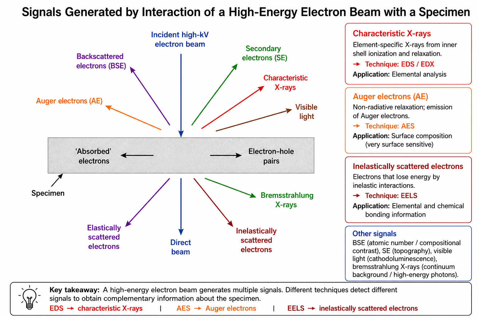
Fig. 27.1 Signals generated by the interaction of a high-energy electron beam with a specimen. EDS exploits the characteristic X-rays; AES exploits the Auger electrons; EELS exploits the inelastically scattered (transmitted) electrons.
The energetics are simple: the incident electron ionises an inner-shell electron (say from the K shell), an outer-shell electron (say from the L shell) fills the vacancy, and the energy difference EK − EL is released as a photon with exactly that energy. Because binding energies are uniquely defined for every element, the X-ray energy is a fingerprint of the emitting atom. In addition to characteristic X-rays, Bremsstrahlung (braking radiation) produces a continuous X-ray background, and Auger electron emission (see Section 3) is a competing de-excitation pathway.
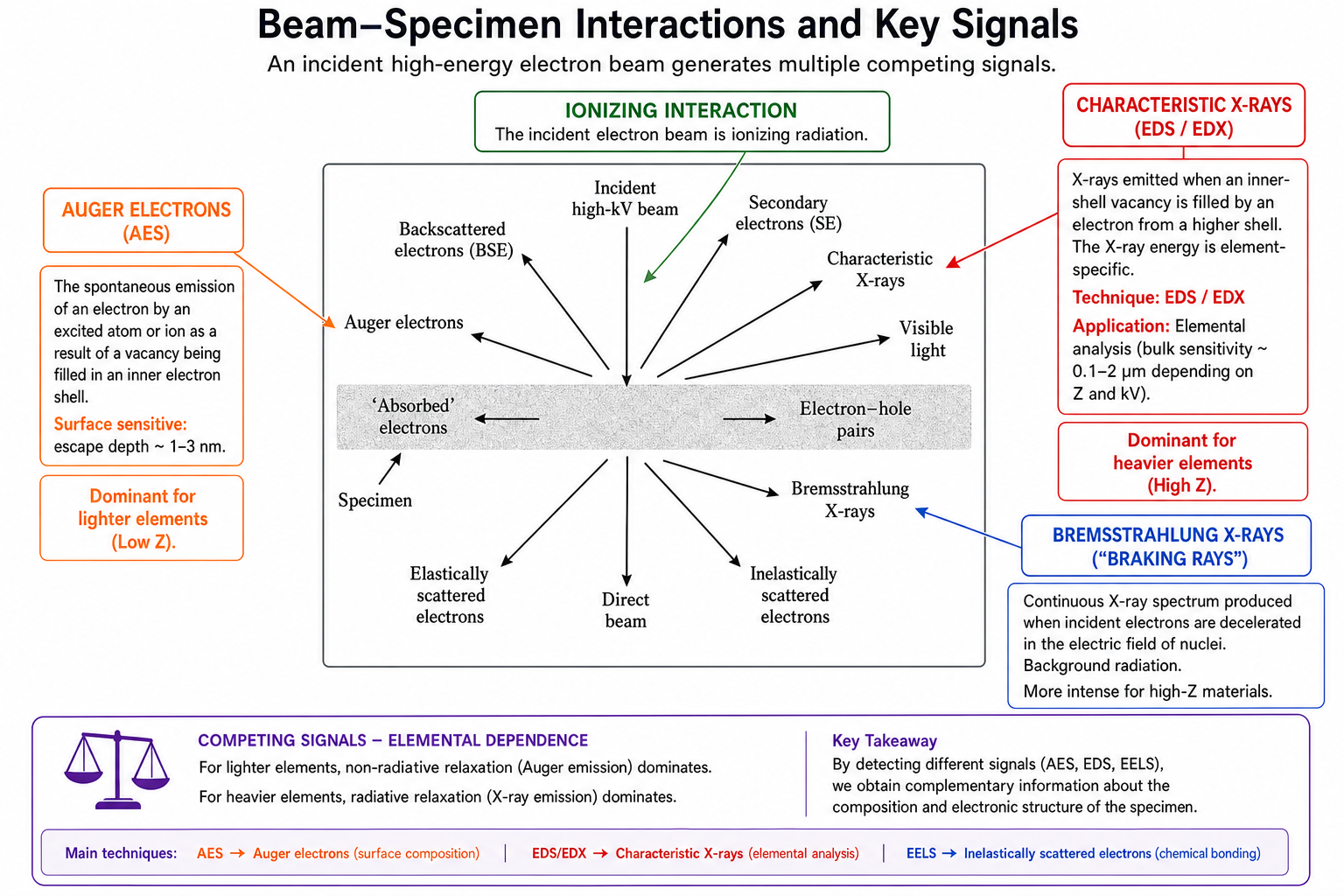
Fig. 27.2 Annotated beam–specimen interaction map highlighting the three competing signals: Auger electrons (surface-sensitive), characteristic X-rays (EDS), and Bremsstrahlung background. Auger emission dominates for lighter elements; X-ray emission dominates for heavier elements.
The spatial resolution of EDS is governed by two factors: the size of the incident electron probe and the volume of material from which the X-rays actually escape. In a bulk SEM specimen the latter is determined by the pear-shaped interaction volume, which can extend 1–3 µm beneath the surface — far larger than the probe itself. In TEM/STEM the specimen is typically 20–200 nm thick, so the interaction volume is dramatically reduced and EDS spatial resolution approaches that of the electron probe.
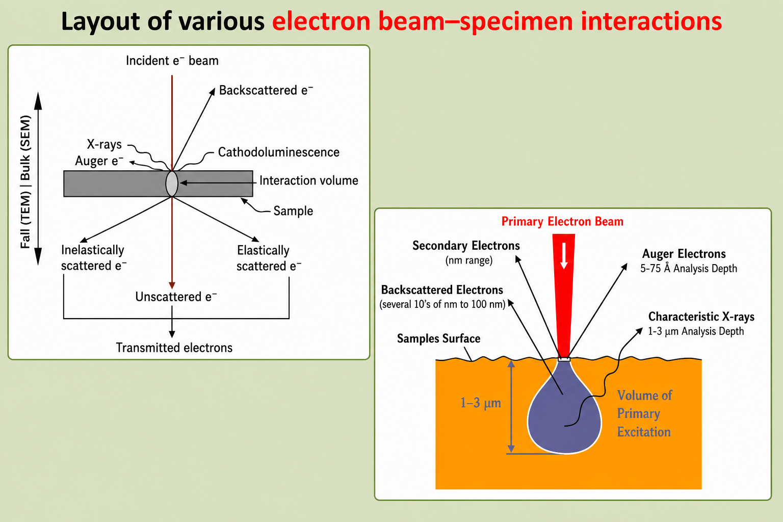
Fig. 27.3 Comparison of electron–specimen interaction volumes for bulk (SEM) and thin (TEM) specimens. The analysis depth of characteristic X-rays (1–3 µm) vastly exceeds that of Auger electrons (5–75 Å), making AES inherently surface-sensitive while EDS in SEM samples a substantial volume. In thin TEM specimens, the interaction volume shrinks dramatically.
3 EDS: Resolution, Electron Guns, and STEM
The spatial resolution of EDS in the SEM is fundamentally limited by the size of the primary electron probe plus the interaction volume. Field emission guns (FEGs) address the probe size part of this equation. Unlike heated tungsten or lanthanum hexaboride (LaB₆) filaments, which are thermal emitters limited by their source brightness, a FEG tip is a sharp tungsten needle subjected to an intense electric field that lowers the surface potential barrier enough for electrons to tunnel out quantum mechanically. The resulting source is far brighter and more coherent, producing a probe of sub-nanometre diameter.
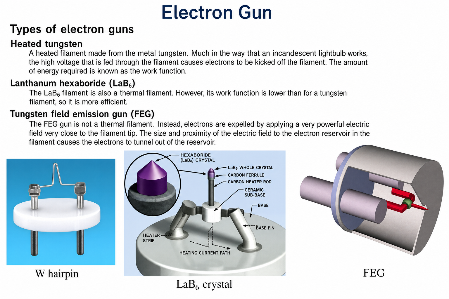
Fig. 27.4 The three main types of electron gun used in electron microscopes. The FEG produces the finest, brightest probe by exploiting quantum tunnelling rather than thermal emission, enabling the highest spatial resolution in both imaging and EDS analysis.
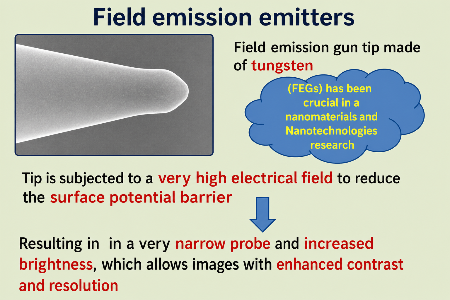
Fig. 27.5 SEM image of a tungsten FEG tip. The atomically sharp apex is subjected to fields of order 10⁹ V/m, sufficient to reduce the surface potential barrier and allow electron tunnelling. The resulting probe has nanometre-scale diameter and high brightness.
For the highest accuracy in nanomaterial EDS, STEM is the preferred platform. In a STEM instrument the specimen is a thin foil (20–200 nm), so the interaction volume through which the beam passes is small compared with a bulk SEM specimen — the beam spreads laterally by only a few nanometres as it traverses the foil. X-ray emission is therefore confined to a correspondingly small column of material. Combined with the sub-ångström probes achievable with aberration correction, this makes STEM-EDS the gold standard for atomic-scale elemental mapping.
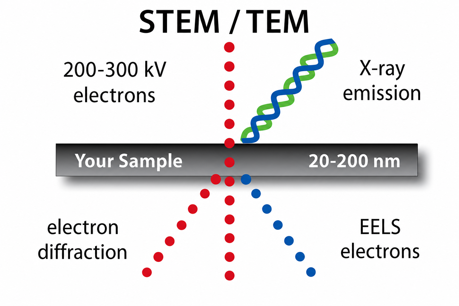
Fig. 27.6 Geometry of EDS in STEM/TEM. The thin specimen (20–200 nm) drastically reduces the interaction volume compared to bulk SEM, greatly improving EDS spatial resolution. The same thin specimen simultaneously allows EELS and electron diffraction.
Aberration correction takes this further still. Spherical aberration in a conventional lens causes electrons far from the optic axis to be focused at a different point than paraxial electrons, spreading the probe. Modern aberration correctors use arrays of multipole lenses to cancel this aberration, reducing probe sizes to sub-ångström dimensions and dramatically improving both spatial resolution and EDS signal localisation.
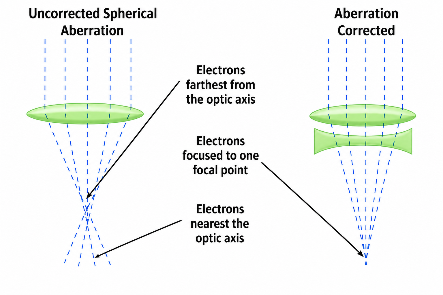
Fig. 27.7 Aberration correction in STEM. Uncorrected spherical aberration causes a spread in focal points (left), limiting probe size. Aberration correction brings all electrons to a single focus (right), reducing probe diameter to sub-ångström and proportionally improving EDS and EELS resolution.
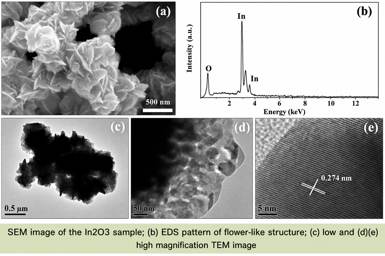
Fig. 27.8 EDS characterisation of flower-like In₂O₃ nanostructures. (a) FESEM morphology; (b) EDS confirms In and O only; (c–e) TEM at increasing magnification shows nanocrystalline grains with resolved lattice fringes (d = 0.274 nm).
4 TEM: Resolution and Accelerating Voltage
Before treating AES and EELS in detail it is worth noting the resolution physics of the TEM platform that hosts both techniques. TEM operates at considerably higher voltages than SEM — typically 120, 200, or 300 kV, with some specialised instruments reaching 1–3 MV. Specimens must be thinned to 50–100 nm because the image is formed by electrons that have been transmitted through the sample, not reflected from its surface.
The theoretical resolution of any wave-optical instrument is governed by the Rayleigh criterion: δ = 0.61λ / (μ sin β), where λ is the wavelength of the illuminating radiation, μ the refractive index of the medium, and β the semi-angle of the objective aperture. The de Broglie wavelength of electrons scales as λ ~ 1.22 / E½ (in Å, with E in eV), so higher accelerating voltages reduce λ and in principle improve resolution. Higher voltages also allow thicker specimens to be studied because the electron mean free path increases. However, in practice the resolution limit of a TEM is set by lens aberrations — primarily spherical aberration — not by the electron wavelength. Aberration correction is therefore the decisive technology for sub-ångström imaging.
5 Auger Electron Spectroscopy (AES)
Auger electron spectroscopy exploits the competing de-excitation pathway to characteristic X-ray emission. After a primary electron ejects a core electron (creating an inner-shell vacancy), an outer-shell electron fills the vacancy — but instead of releasing the energy as an X-ray photon, the atom can transfer that energy to a third electron in another outer shell, which is then ejected. This ejected electron is called an Auger electron. Its kinetic energy is characteristic of the element because it equals the difference between the binding energies of the shells involved, minus the binding energy of the emitted electron's own shell.
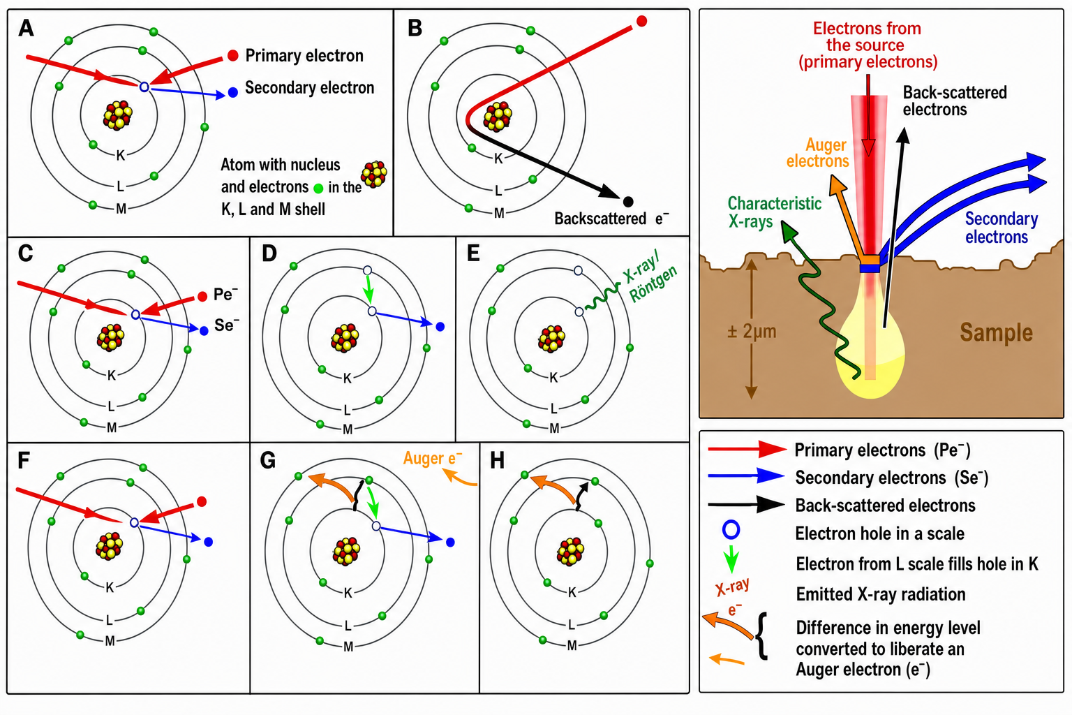
Fig. 27.9 Comparison of the EDS (X-ray emission, panels A–E) and AES (Auger electron emission, panels F–H) processes at the atomic level. In EDS, the energy released when an outer-shell electron fills an inner-shell vacancy is emitted as a characteristic X-ray photon. In AES, that energy is instead transferred to a third electron (the Auger electron), which is ejected. Both energies are element-specific.
The three-step Auger process is conventionally named by the shells involved. If a K-shell electron is initially ejected, an L₁-shell electron fills the vacancy, and the released energy ejects an L₂-shell electron, the process is called a KL₁L₂ Auger process. The Auger kinetic energy is approximately EKL₁L₂ ≈ EK − EL₁ − EL₂. Since these binding energies are unique to each element, the Auger electron energy is a fingerprint of the emitting atom. AES therefore provides elemental identification from the measured kinetic energy distribution of emitted electrons.
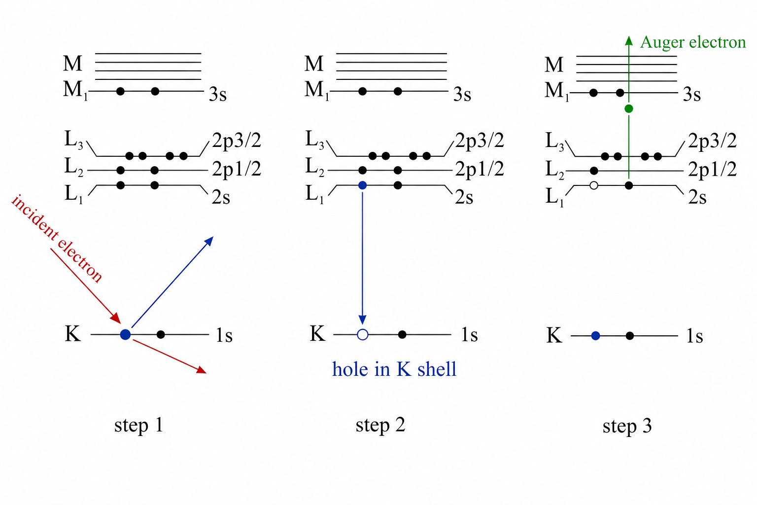
Fig. 27.10 The three steps of the KL₁L₂ Auger process. (1) Incident electron ejects a K-shell (1s) electron. (2) The K-shell vacancy is filled by an L₁ (2s) electron. (3) The energy released in step 2 is transferred to an L₂ (2p₁/₂) electron, which is ejected as the Auger electron — with a kinetic energy equal to EK − EL₁ − EL₂.
6 AES: Properties, Advantages, and Limitations
The primary electrons used to initiate Auger transitions typically have energies in the range 3–20 keV and must be incident on a conducting sample to prevent charging. AES is uniquely useful for chemical characterisation of thin films, surfaces, and interfaces because it is inherently surface-sensitive — and this sensitivity arises from the physics of Auger electron escape, not from the depth of the primary ionisation event.
Although the primary beam can ionise atoms tens of nanometres below the surface, only Auger electrons generated very close to the surface can escape without losing energy through inelastic collisions on their way out. Auger electrons typically have kinetic energies in the range 50–2000 eV; at 1000 eV the inelastic mean free path in most materials is only about 15 Å. This means the observation depth — the depth from which Auger electrons carry useful compositional information — is only about 15 Å, and typical probing depths are in the range 10–30 Å.
Beyond elemental identification at surfaces, AES is used to study film growth kinetics, surface chemical composition (elemental analysis and mapping), and depth profiling — a technique in which the surface is progressively sputtered away by an ion beam while AES spectra are continuously recorded, revealing the concentration of each element as a function of depth. This is particularly powerful for characterising multilayer thin film structures.
The principal disadvantage of AES is beam damage. Because high-energy and high-current-density primary electron beams are required to produce measurable Auger signals, defects are generated in the sample at relatively high density. This is a serious concern for radiation-sensitive materials such as biological specimens, polymers, and some oxide nanostructures.
7 AES: Experimental Example
The element-specificity of Auger electron kinetic energies is demonstrated directly by experiment. The figure below shows two AES spectra in the derivative mode (dN/dE vs E), which is the standard presentation because it enhances the visibility of the small Auger peaks superimposed on a large secondary-electron background.
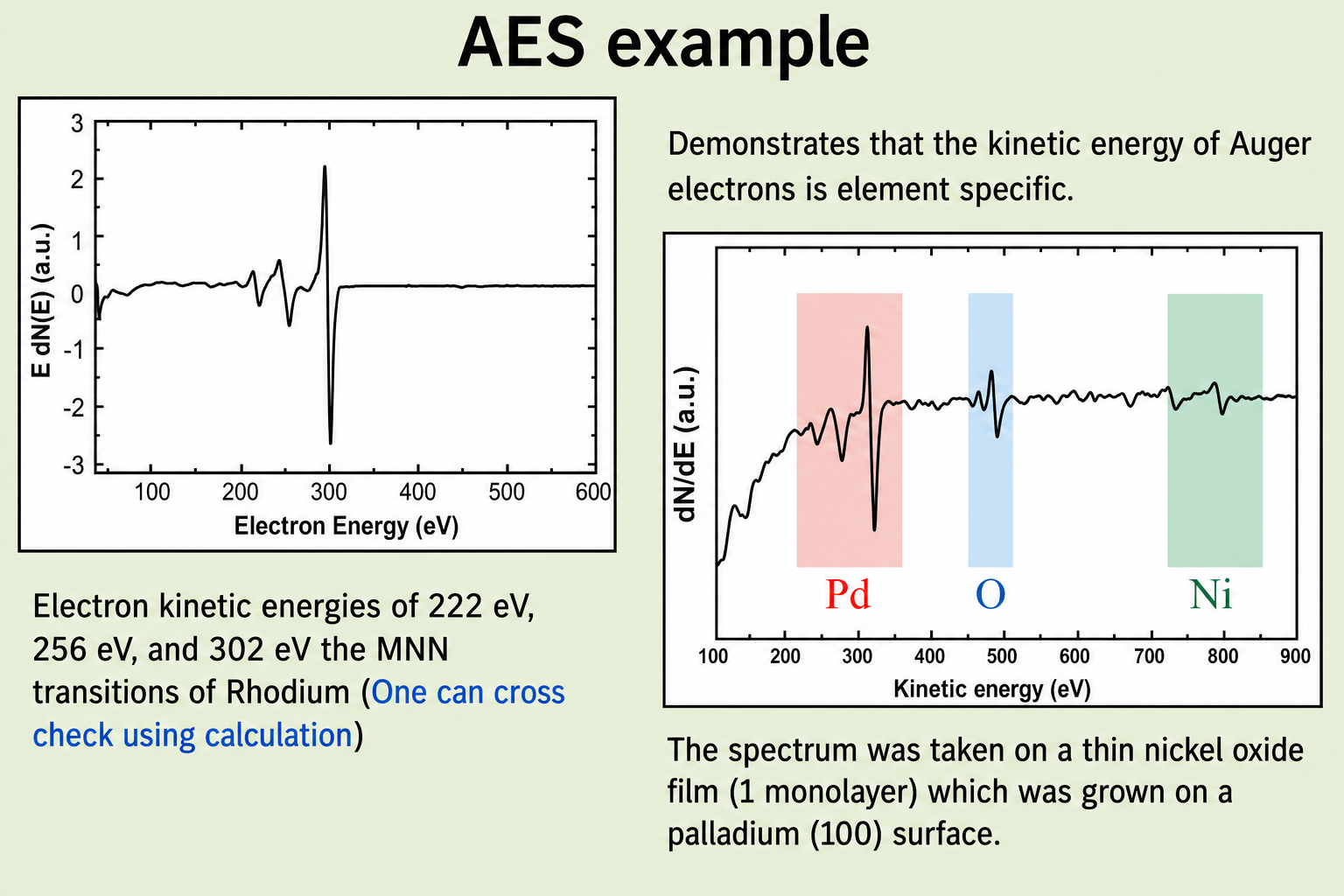
Fig. 27.11 AES derivative spectra demonstrating element-specific Auger electron kinetic energies. Left: Rhodium MNN transitions at 222, 256, and 302 eV. Right: thin NiO film on Pd(100) — peaks from all three elements (Pd, O, Ni) are resolved at their characteristic energies, confirming surface composition.
In the left spectrum, three peaks at 222 eV, 256 eV, and 302 eV correspond to the MNN Auger transitions of Rhodium — the exact energies predicted from the binding energies of Rhodium's M and N shells. In the right spectrum, taken from a monolayer of nickel oxide grown epitaxially on a palladium (100) single-crystal surface, peaks from all three elements (Pd, O, Ni) are resolved at their respective characteristic energies. This demonstrates both the surface sensitivity of AES (it detects the single-monolayer NiO overlayer) and its ability to identify multiple elements simultaneously.
8 Electron Energy Loss Spectroscopy (EELS)
EELS is performed almost exclusively in TEM and STEM instruments, where the thin specimen allows the transmitted electron beam to be collected after it has passed through the sample. The principle is to measure the energy that electrons lose during inelastic collisions with the specimen. An electron entering with a precisely defined kinetic energy E₀ can lose energy through a variety of mechanisms — plasmon excitation, single-electron interband transitions, and core-level ionisation. Each mechanism leaves a characteristic imprint on the energy distribution of the transmitted beam, which is measured by dispersing the beam in a magnetic prism spectrometer and detecting it on a CCD.
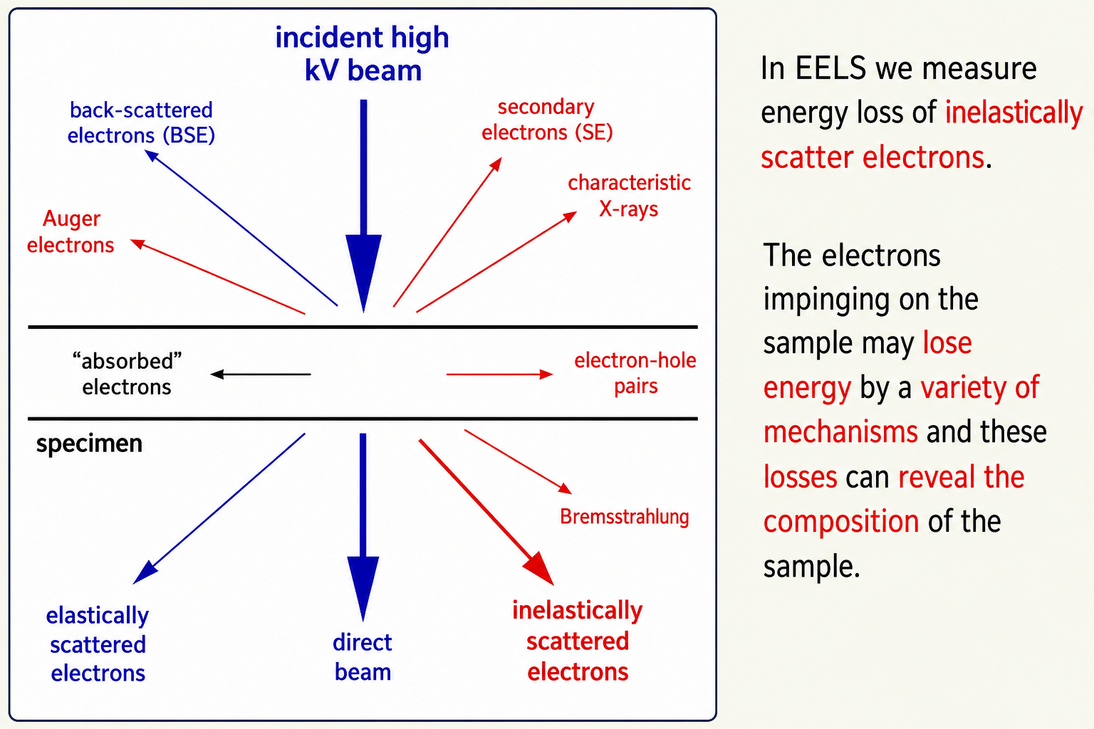
Fig. 27.12 EELS probes the inelastically scattered electrons that pass through the thin TEM specimen. While EDS captures X-rays emitted above the specimen, EELS analyses the energy distribution of transmitted electrons that have lost discrete amounts of energy to specific inelastic interactions.
After passing through the magnetic prism, the transmitted electrons are spread by energy and focused onto a detector. Electrons that retained their full energy (elastically scattered or unscattered) form the zero-loss peak — the most intense feature, carrying no compositional information but useful for calibration and measuring specimen thickness. The remaining electrons, which have lost discrete amounts of energy, form the EELS spectrum proper.
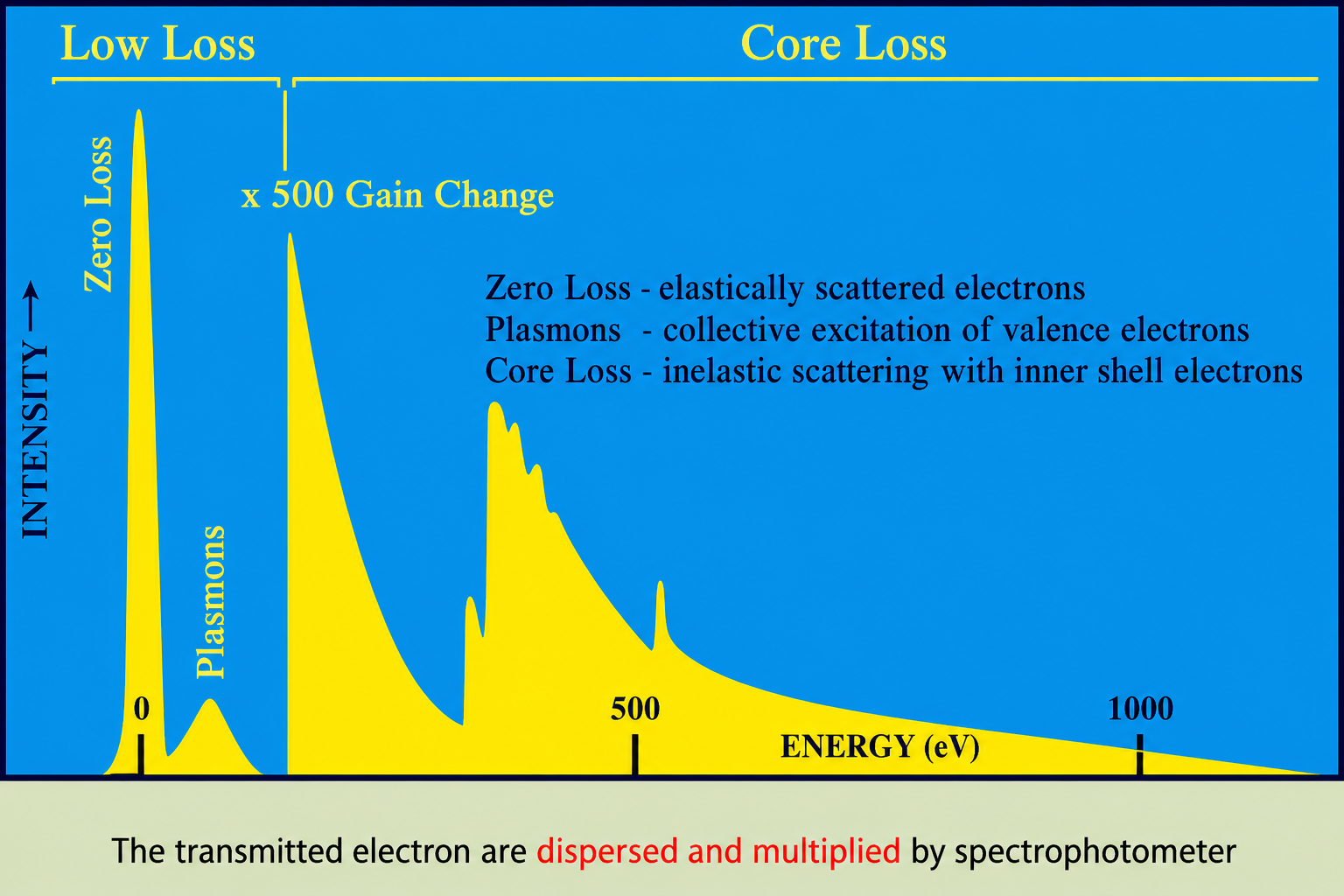
Fig. 27.13 A typical EELS spectrum showing all three regions. The zero-loss peak (elastic electrons) dominates at 0 eV. The low-loss region (0–50 eV) contains plasmon peaks. The core-loss region (above ~50 eV) contains element-specific ionisation edges. A ×500 gain change is applied to make the low- and core-loss features visible.
9 The EELS Spectrum: Three Regions
The EELS spectrum is conventionally divided into three regions, each arising from a distinct class of electron–specimen interaction.
Region 1 — Zero-loss region (0–10 eV): This region is dominated by the zero-loss peak, which contains electrons that have not undergone any measurable inelastic scattering. These electrons carry no compositional information but are used for instrument calibration and — through the ratio of zero-loss intensity to total spectral intensity — for measuring specimen thickness.
Region 2 — Low-loss region (10–60 eV): This region reflects excitation of plasmons and interband transitions. Plasmons are collective oscillations of the valence electron gas: the entire free-electron sea oscillates in response to the passing fast electron, losing energy in quantised amounts called plasmon quanta, typically 5–30 eV for metals and semiconductors. Plasmon losses are the most frequent cause of energy loss in EELS spectra. Their intensity scales with specimen thickness, so the low-loss region can be used to estimate thickness.
![Low-loss EELS spectrum on the left showing a sharp zero-loss peak and a broader low-loss plasmon peak at 0–80 eV with x-axis labelled E[eV]. Text annotations state: 1) it is the region with energy losses up to 50 eV; 2) it reflects excitation of plasmons and interband transitions. Below: plasmon losses are a frequent cause of energy loss; plasmons are collective excitations of the electron gas and are typically several electron Volts in magnitude.](nano_images/lec27_fig14.jpg)
Fig. 27.14 The low-loss region of an EELS spectrum, showing the sharp zero-loss peak followed by the broader plasmon peak. The zero-loss peak records elastically scattered electrons (no information); the plasmon peak arises from collective valence electron oscillations and its intensity is proportional to specimen thickness.
Region 3 — Core-loss region (above ~60 eV): This is the analytically valuable region. Energy losses above ~50 eV correspond to inelastic scattering events in which the incident electron has transferred enough energy to excite a core electron (inner-shell electron) to an unoccupied state above the Fermi level. The onset of each such excitation appears as a characteristic edge in the spectrum — an abrupt increase in intensity at the binding energy of the relevant core level, followed by a gradually decaying tail. Because core-level binding energies are element-specific, each edge identifies an element.
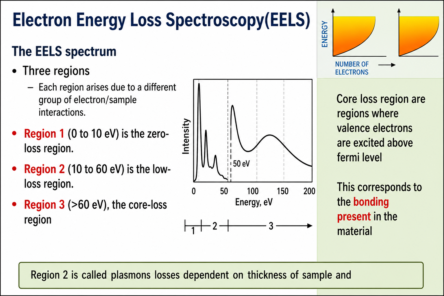
Fig. 27.15 The full EELS spectrum with all three regions identified. The core-loss region (Region 3, >60 eV) contains element-specific ionisation edges; the fine structure of these edges reflects the unoccupied density of states and hence bonding. The low-loss region (Region 2) shows plasmon peaks whose spacing and intensity encode specimen thickness.
The region of the spectrum used in quantitative EELS analysis is therefore above 50 eV, where core-loss edges rise above the steeply decaying background of plasmon losses. Each element produces edges at its characteristic core-level binding energies, and the intensity under each edge is proportional to the number of atoms of that element in the beam path — enabling quantitative elemental analysis.
10 Core-Loss Edges: Absorption Edges and Fine Structure
The fine structure near a core-loss edge in EELS carries far more information than simply the edge onset energy. The electron energy-loss near-edge structure (ELNES) — the detailed shape of the edge in the 0–30 eV window above onset — reflects the unoccupied density of states into which the core electron is excited. Because the available unoccupied states are determined by the bonding environment of the atom, ELNES is sensitive to chemical bonding, oxidation state, coordination geometry, and hybridisation.
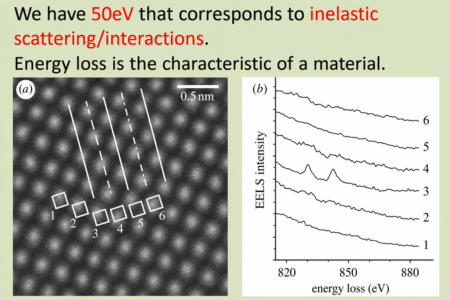
Fig. 27.16 Atomic-column-resolved EELS. The STEM image (a) shows individual atomic columns; EELS spectra (b) acquired from each numbered column show that the core-loss edge at ~880 eV is localised in specific columns (columns 3–4), demonstrating that STEM-EELS can map elemental identity at the single-atom-column level.
A classic illustration of ELNES sensitivity comes from the carbon allotropes. Diamond, graphite, C60 fullerene, and amorphous carbon all consist only of carbon atoms, yet their EELS spectra are dramatically different. All show a prominent edge near 284 eV — the K-shell ionisation edge of carbon. However, graphite and fullerene show a sharp pre-edge feature at ~285 eV corresponding to the excitation of a 1s (K-shell) core electron to an empty π* anti-bonding orbital. This feature is entirely absent in diamond because diamond has no π electrons — all carbon atoms are sp³-hybridised with purely σ bonds. The presence or absence of the π* peak is therefore a direct fingerprint of sp² versus sp³ carbon bonding.
![EELS spectra of three carbon allotropes on a yellow background. X-axis: Loss Energy [eV] from 280 to 360. Y-axis: intensity. Three overlaid curves labelled Graphite (pink/red, top), C60 (pink/red, middle), and Diamond (blue, bottom). A vertical purple line marks 284 eV. A sharp pre-edge peak at ~285 eV (labelled 1s→π*) is prominent in graphite and C60 but absent in diamond. Inset crystal structure diagrams for graphite (layered hexagonal), C60 (buckyball), and diamond (tetrahedral). Caption: all specimens have absorption peaks around 284 eV corresponding to carbon atoms; fine structure of the absorption peak reveals bonding state and local electronic state; sharp peak at absorption edge corresponds to excitation of 1s electron to empty anti-bonding π-orbital; not observed for diamond because of no π-electron.](nano_images/lec27_fig17.jpg)
Fig. 27.17 EELS spectra of graphite, C60 and diamond. All show the carbon K-edge near 284 eV. The 1s→π* pre-edge peak at ~285 eV is present in graphite and C60 (sp² carbon, π bonds) but absent in diamond (sp³ carbon, no π electrons). This fine-structure difference allows EELS to distinguish carbon bonding types at nanometre spatial resolution.
11 Absorption Edges and Specimen Thickness Effects
The concept of absorption edges is central to interpreting core-loss EELS. When an incident photon or electron transfers enough energy to a core electron to promote it above the vacuum level, the atom is ionised — the core electron escapes entirely. This threshold energy, called the absorption edge, is the onset of inner-shell ionisation. Above the edge onset, the excited core electron can be promoted to either a short-lived excited bound state or an ionised state, leading to the characteristic sawtooth-shaped edge in the EELS spectrum.
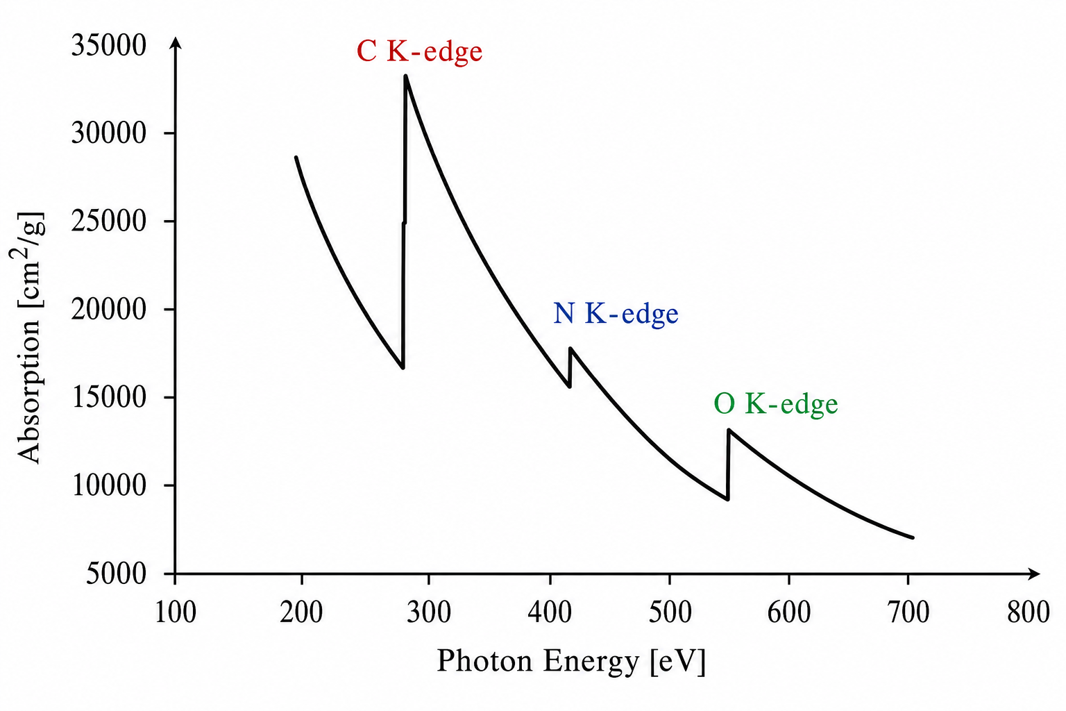
Fig. 27.18 Absorption edges for carbon, nitrogen, and oxygen. Each edge marks the onset of inner-shell ionisation at the binding energy of the respective K shell (C at ~284 eV, N at ~400 eV, O at ~530 eV). The sharp onset followed by a gradual decay is the characteristic shape of an inner-shell ionisation edge.
A critical practical complication in EELS is specimen thickness. Plasmon losses always appear in the EELS spectrum of any specimen thicker than a few nanometres; their intensity scales with thickness because each plasmon scattering event has a fixed mean free path (typically 50–100 nm in most materials). For thin specimens the low-loss spectrum shows a single plasmon peak; for thicker specimens multiple plasmon losses accumulate, producing a series of peaks at multiples of the plasmon energy. When the specimen becomes too thick (beyond ~50–100 nm, or roughly one mean free path), these multiple scattering events convolute with the core-loss signal and make quantitative analysis unreliable.
![Two EELS low-loss spectra comparing thin and thick specimens. Left spectrum (thin): a tall zero-loss peak I₀ and a single smaller plasmon peak Ip at ~15 eV; the rest of the spectrum (20–140 eV) is flat. Right spectrum (thick): I₀ remains large, but now Ip is large and additional peaks Ip2 and Ip3 appear at ~30 eV and ~45 eV due to double and triple plasmon scattering. X-axis: E[eV] from 0 to 140. Caption: in the EELS spectra, plasmon losses always occur except for ultra-thin specimens; thus used to estimate specimen thickness; when the specimen is quite thick, multiple plasmon losses make straightforward analysis impossible.](nano_images/lec27_fig19.jpg)
Fig. 27.19 Thickness effects in EELS. Left: a thin specimen shows a single plasmon peak Ip. Right: a thicker specimen shows multiple plasmon peaks (Ip, Ip₂, Ip₃) from successive plasmon scattering events. The ratio I₀/(I₀+Ip) can be used to estimate specimen thickness; specimens thicker than ~50 nm make EELS analysis unreliable due to multiple scattering.
12 Comparing EDS, AES, and EELS
The three electron spectroscopies are complementary rather than competing. Choosing the right technique depends on the question being asked, the specimen type, and the available instrumentation.
Spatial resolution: EELS has the highest spatial resolution of the three. When combined with aberration-corrected STEM, EELS can map elemental composition and bonding at the single-atom-column level. EDS spatial resolution in SEM is limited by the interaction volume to ~1 µm; in STEM it approaches the probe size (~0.1 nm). AES spatial resolution is limited by the primary beam diameter to ~5–10 nm in modern instruments.
Energy resolution: EELS achieves ~0.1–0.3 eV energy resolution with a cold FEG source and monochromator — far better than EDS (~100–130 eV resolution). This allows EELS to resolve chemical shifts, bonding information, and the fine structure of edges. AES energy resolution is intermediate (~1 eV).
Light element sensitivity: EELS is superior for detecting light elements (H, Li, Be, B, C, N, O) because their K-shell edges fall in the accessible EELS energy range and their X-ray yields (for EDS) are very low. AES also detects light elements well. EDS struggles with elements lighter than sodium (Z < 11) due to low fluorescence yield and X-ray absorption.
Electronic structure information: Only EELS provides direct access to the unoccupied density of states through near-edge fine structure (ELNES). This allows bonding state, hybridisation, and oxidation state to be determined — information unavailable from EDS or AES.
Ease of use: EDS is the easiest to use and fastest for routine qualitative composition analysis. The spectrum is straightforward to interpret and the required detector is standard equipment on most SEM and TEM instruments. EELS requires thinner specimens, more careful data acquisition, and more sophisticated analysis. AES requires ultra-high vacuum and conducting specimens.
✦ References & Further Reading
- Williams, D. B. & Carter, C. B. (2009). Transmission Electron Microscopy: A Textbook for Materials Science (2nd ed.). Springer. [Comprehensive treatment of EDS and EELS in TEM.]
- Egerton, R. F. (2011). Electron Energy-Loss Spectroscopy in the Electron Microscope (3rd ed.). Springer. [The definitive EELS reference.]
- Brydson, R. (2001). Electron Energy Loss Spectroscopy. Bios Scientific Publishers.
- Briggs, D. & Seah, M. P. (Eds.) (1990). Practical Surface Analysis: Auger and X-ray Photoelectron Spectroscopy (2nd ed.). Wiley.
- Goldstein, J. I. et al. (2018). Scanning Electron Microscopy and X-Ray Microanalysis (4th ed.). Springer. [Standard SEM-EDS reference.]
- Pennycook, S. J. & Nellist, P. D. (Eds.) (2011). Scanning Transmission Electron Microscopy: Imaging and Analysis. Springer.
Key Takeaways
- EDS detects characteristic X-rays emitted when inner-shell vacancies are filled after electron-beam ionisation; gives rapid elemental identification with ~1 µm spatial resolution in SEM and sub-nanometre in STEM.
- AES measures kinetic energies of Auger electrons — the radiationless de-excitation alternative — and is uniquely surface-sensitive (probing depth 10–30 Å), ideal for thin films and depth profiling despite beam-damage risk.
- EELS analyses energy losses of transmitted electrons, achieving the highest spatial and energy resolution of all three techniques and uniquely revealing electronic structure and chemical bonding via near-edge fine structure.
- Together, EDS, AES, and EELS form a comprehensive chemical characterisation toolkit covering spatial scales from micrometres down to individual atomic columns.
Carbon Nanotubes: Structure, Chirality & Applications
From the graphene lattice to the chiral vector — how the geometry of rolling determines whether a nanotube conducts like a metal or a semiconductor, and why that makes CNTs uniquely useful for nanoelectronics, composites, and beyond.
Contents
- Why Carbon Nanotubes?
- Geometry: A Rolled Graphene Sheet
- Single-Walled and Multi-Walled CNTs
- The Chiral Vector: Defining Nanotube Type
- Armchair, Zigzag, and Chiral Nanotubes
- Why Chirality Matters: The CNT Zoo
- Extraordinary Properties of CNTs
- Synthesis Methods
- Discovery: Iijima and the Arc Discharge Story
- CNTs for Nanoelectronic Interconnects
- CNT Composites
- Silicon Photolithography: CNT Integration Context
- References & Further Reading
1 Why Carbon Nanotubes?
Carbon nanotubes occupy a singular position in nanomaterials science because they combine extraordinary properties across multiple domains — mechanical, electrical, and thermal — in a single one-dimensional structure. This combination arises directly from their architecture: a seamless cylinder of sp²-hybridised carbon, effectively a strip of graphene rolled into a tube. The same strong in-plane σ bonds that make graphite hard along its basal plane and diamond the hardest natural material become the load-bearing backbone of the nanotube wall.
Current applications already span AFM probe tips, scaffold materials for bone growth, lightweight bicycle components, wind turbine blades, marine paints, and conductive polymer composites. All of these interfaces with the natural and built environment raise questions about environmental and health impacts that remain an active area of investigation.
2 Geometry: A Rolled Graphene Sheet
The mental model for a CNT is simple: take a single sheet of graphene — the flat, honeycomb-lattice monolayer of carbon — and roll it into a seamless cylinder. The two models below show, on the left, a rendered graphene sheet with its multilayer stacking (as found in graphite), and on the right, a ball-and-stick model of the resulting single-walled nanotube. Every carbon atom remains threefold-coordinated and sp²-hybridised; the only structural change is the curvature introduced by rolling.
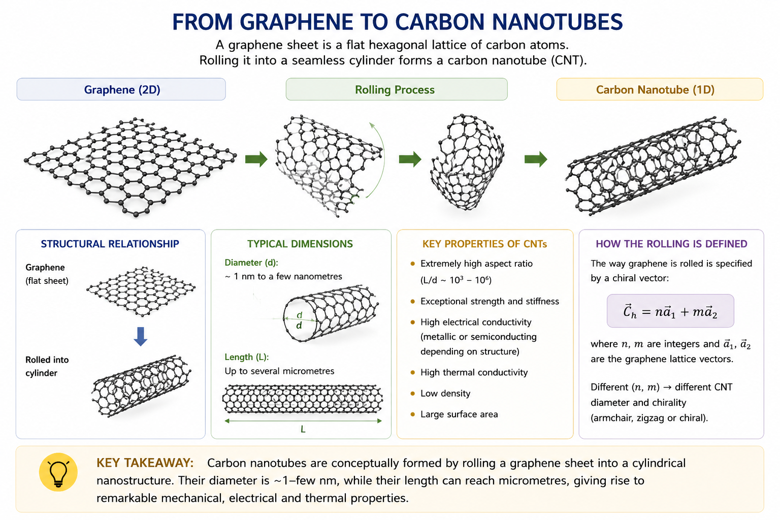
Fig. 28.1 The conceptual relationship between graphene and a carbon nanotube. A graphene sheet (left) is a flat hexagonal carbon lattice; rolling it into a seamless cylinder (right) produces a CNT. The nanotube diameter ranges from ~1 nm to a few nanometres, and its length can reach micrometres.
CNTs are cylindrical molecules with a diameter ranging from 1 nm to a few nanometres and length up to a few micrometres. The small diameter places them squarely in the quantum-confinement regime perpendicular to the tube axis, while the long axis remains essentially classical. This dimensional asymmetry is responsible for nearly every unusual property they possess.
3 Single-Walled and Multi-Walled CNTs
Two broad structural classes are recognised. A single-walled carbon nanotube (SWCNT) consists of a single cylindrical graphene shell. Its electronic character — metallic or semiconducting — depends sensitively on how the graphene sheet was rolled, quantified by the chiral indices (n, m) discussed in the next section. SWCNTs typically have diameters of 0.7–2 nm.
A multi-walled carbon nanotube (MWCNT) consists of two or more concentric graphene cylinders, with an interlayer spacing of ~0.34 nm (matching the interlayer spacing of graphite). Because the multiple shells present a range of chiralities, their combined electronic structure always gives a metallic character — MWCNTs are always metallic, regardless of their outer diameter or how they were grown.
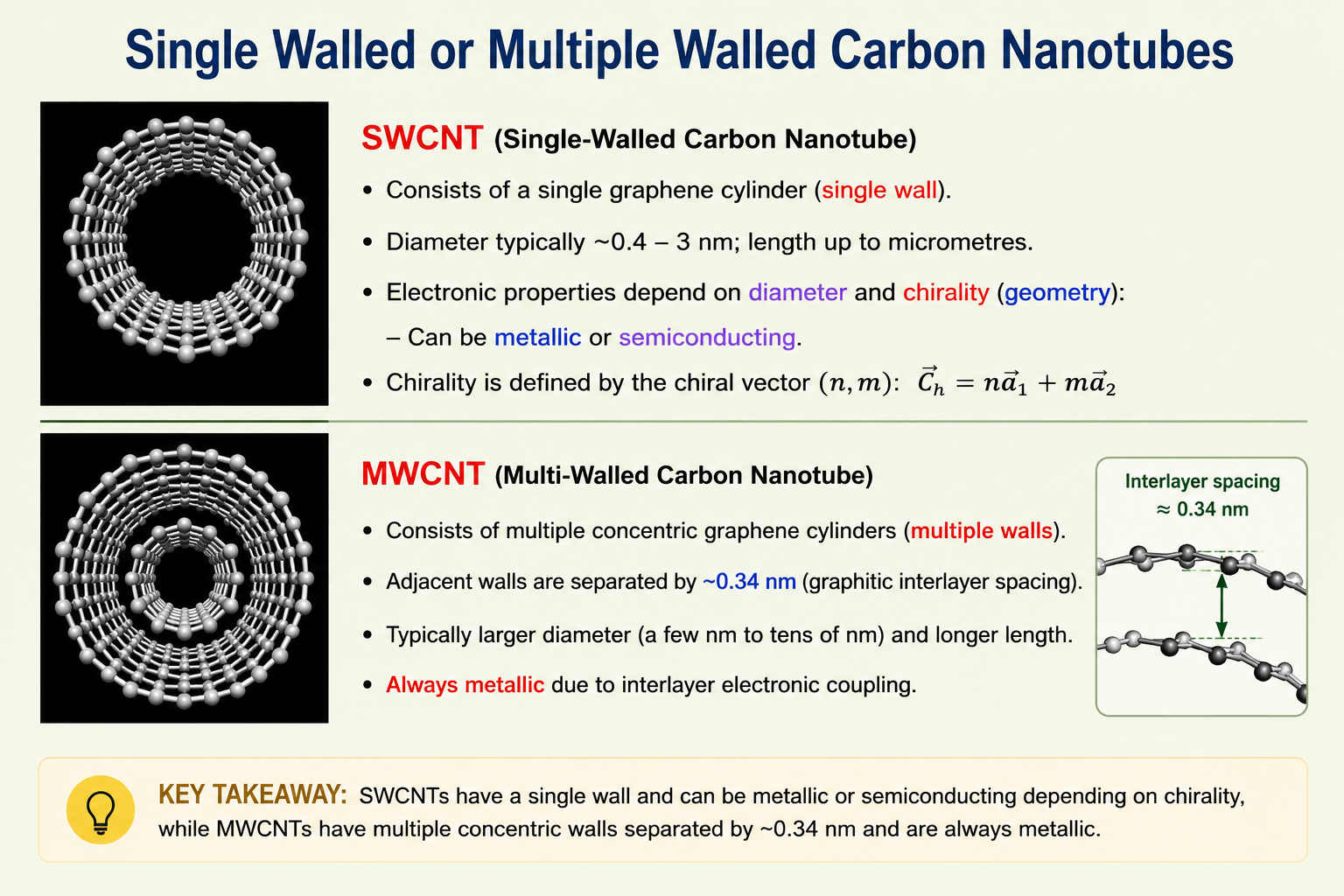
Fig. 28.2 End-on views of a single-walled CNT (top) and a multi-walled CNT (bottom). The SWCNT has one graphene shell; the MWCNT has concentric shells separated by ~0.34 nm. SWCNTs can be metallic or semiconducting depending on chirality; MWCNTs are always metallic.
4 The Chiral Vector: Defining Nanotube Type
The electronic properties of an SWCNT are entirely determined by the direction in which the graphene sheet is rolled — its chirality. This direction is specified by the chiral vector R = na₁ + ma₂, where a₁ and a₂ are the two primitive lattice vectors of the graphene hexagonal lattice and n, m are non-negative integers. The chiral vector points from one carbon atom to the atom that coincides with it when the sheet is rolled into a cylinder.
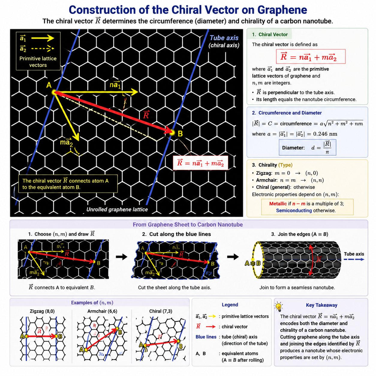
Fig. 28.3 Construction of the chiral vector on an unrolled graphene lattice. The two blue lines define the tube axis; cutting along these lines and joining the edges forms the nanotube. The chiral vector R (red) connects atom A to the equivalent atom B, encoding both the diameter and the chirality. The yellow vectors na₁ and ma₂ are its components along the primitive lattice directions.
To construct the chiral vector geometrically: imagine the nanotube is unrolled into a planar strip. Draw two parallel lines (the blue lines) along the tube axis to mark where the cut-and-join takes place. Any carbon atom on one blue line (point A) maps onto a carbon atom on the other (point B) when the sheet is re-rolled. The vector from A to B is the chiral vector R. The wrapping angle Φ is the angle between R and the armchair line — the line that bisects each hexagon across the midpoints of opposite bonds.
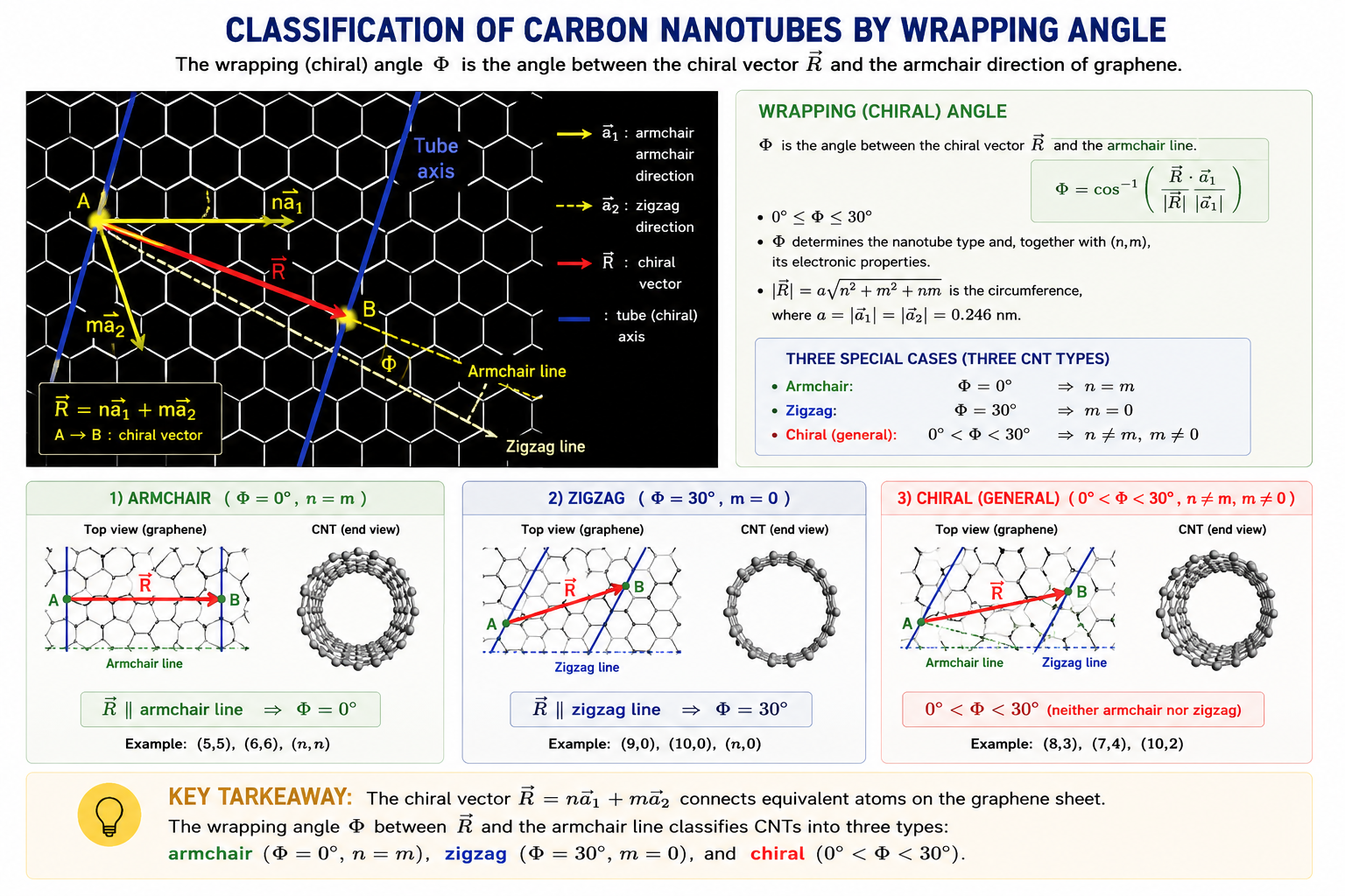
Fig. 28.4 Classification of CNTs by the wrapping angle Φ between the chiral vector R and the armchair line. Three special cases define the three nanotube types: armchair (Φ = 0°, n = m), zigzag (Φ = 30°, m = 0), and chiral (0° < Φ < 30°).
5 Armchair, Zigzag, and Chiral Nanotubes
Three distinct tube types arise from the chirality classification, each with characteristic electronic properties:
Armchair (n, n): The chiral vector lies along the armchair direction (Φ = 0°, so m = n). Armchair nanotubes have a metallic band structure with no gap at the Fermi level. They are the most conductive CNT type and are therefore the preferred target for interconnect applications.
Zigzag (n, 0): The chiral vector lies along the zigzag direction (Φ = 30°, so m = 0). Zigzag tubes have a finite band gap between the highest occupied and lowest empty electronic states — they behave as semiconductors (or narrow-gap metals depending on the exact index n).
Chiral (n, m): All other tubes, where both n and m are arbitrary integers and 0 < Φ < 30°. Their electronic character depends on the specific values of (n, m): a tube is metallic if (n − m) is divisible by 3, and semiconducting otherwise.
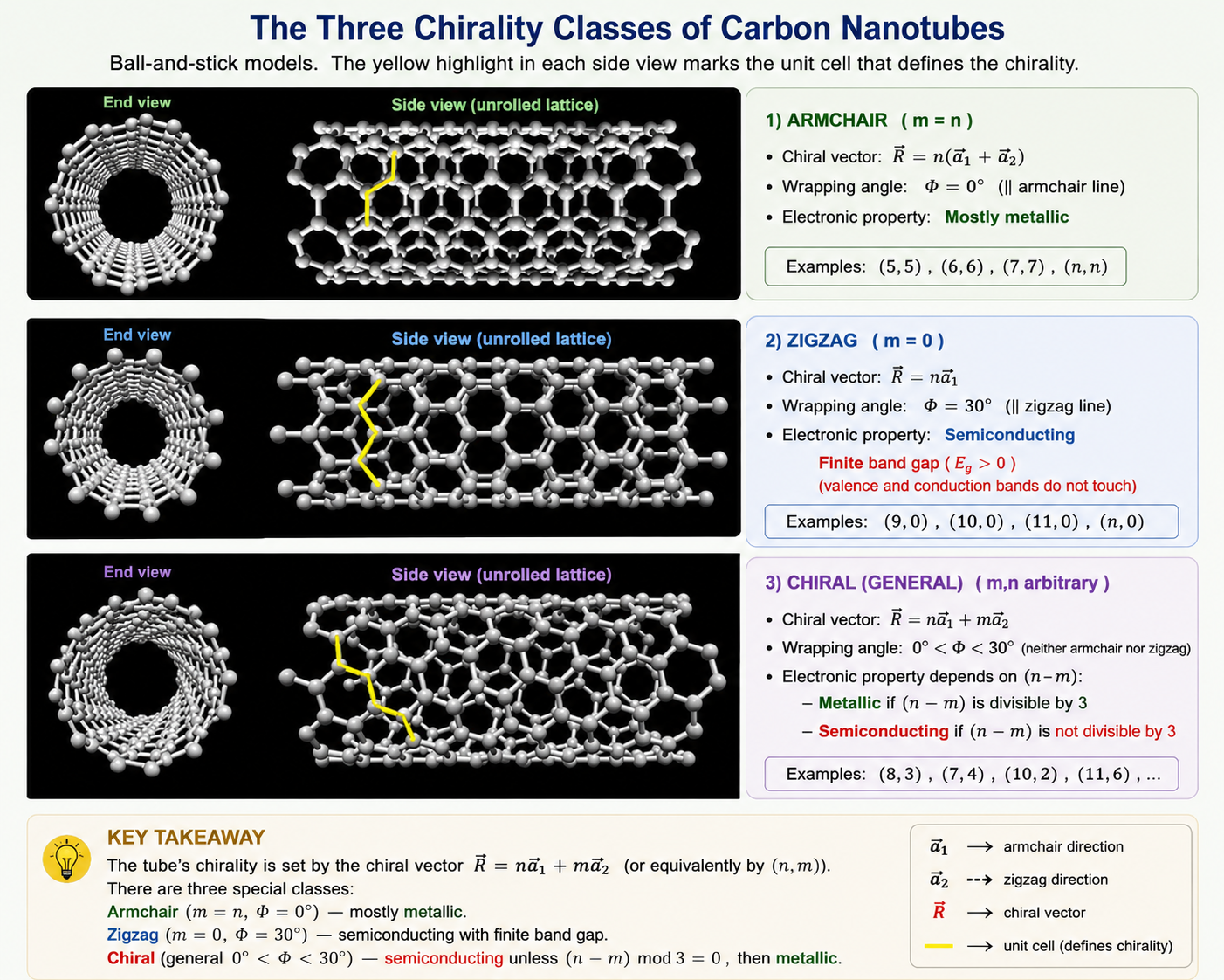
Fig. 28.5 Ball-and-stick models of the three CNT chirality classes. Armchair (top, m = n): metallic. Zigzag (middle, m = 0): semiconducting, finite band gap. Chiral (bottom, m,n arbitrary): semiconducting when (n − m) is not divisible by 3, metallic otherwise. The yellow highlight in each side-on view marks the unit cell that defines the chirality.
6 Why Chirality Matters: The CNT Zoo
The profound consequence of chirality is that a SWCNT with (5,5) indices is a metal, while one with (10,5) indices is a semiconductor — despite being made from exactly the same atoms. This sensitivity arises from quantum confinement: the circumferential boundary condition forces the transverse wavevectors to take only discrete values (quantum confinement), and whether one of those allowed values lands exactly at the K-point of the graphene Brillouin zone — where the conical band-crossing occurs — determines the band gap.
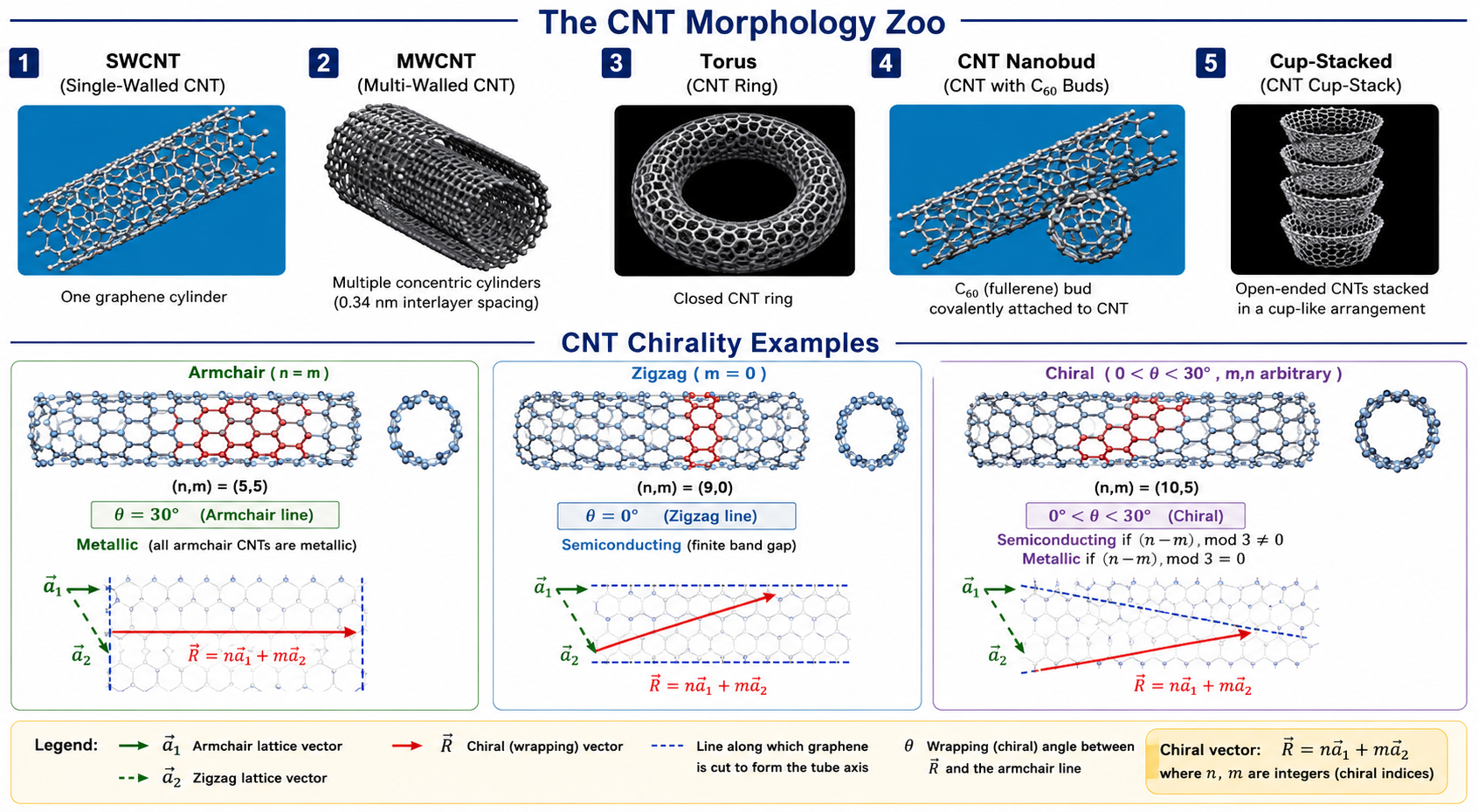
Fig. 28.6 The CNT morphology zoo (top row) and chirality examples (bottom row). Beyond the standard SWCNT and MWCNT, variants include the torus (closed ring), CNT nanobud (nanotube with C₆₀ buds), and cup-stacked geometry. The bottom row shows atomic-scale models of the three chirality types with their (n,m) indices and wrapping angles.
7 Extraordinary Properties of CNTs
The combination of the strong C–C σ bond network and the quasi-1D geometry gives CNTs a property profile unmatched by any other material:
Mechanical: The Young's modulus of SWCNTs is approximately 1 TPa along the tube axis — roughly five times that of steel and comparable to diamond. For reference, tungsten (one of the stiffest metals) has a modulus of ~411 GPa. CNTs can endure tensile stresses of ~30 GPa before failure, also far exceeding tungsten (~~2 GPa).
Electrical: Metallic SWCNTs and MWCNTs carry current densities up to 10⁹ A/cm², four orders of magnitude higher than a copper wire (which fails by electromigration above ~10⁵ A/cm²). This extraordinary current density results from ballistic electron transport — electrons propagate along the tube axis without phonon or impurity scattering, because all transverse electronic states are quantised and the relevant scattering mechanisms are suppressed.
Thermal: The thermal conductivity of SWCNTs along the tube axis is estimated at ~3000–6000 W/mK, far exceeding copper (~400 W/mK) and aluminium (~205 W/mK). Again, the near-defect-free structure and ballistic phonon transport underpin this value.
8 Synthesis Methods
Three main techniques are used to grow CNTs. They differ in the type of nanotube produced, the achievable quality, and cost:
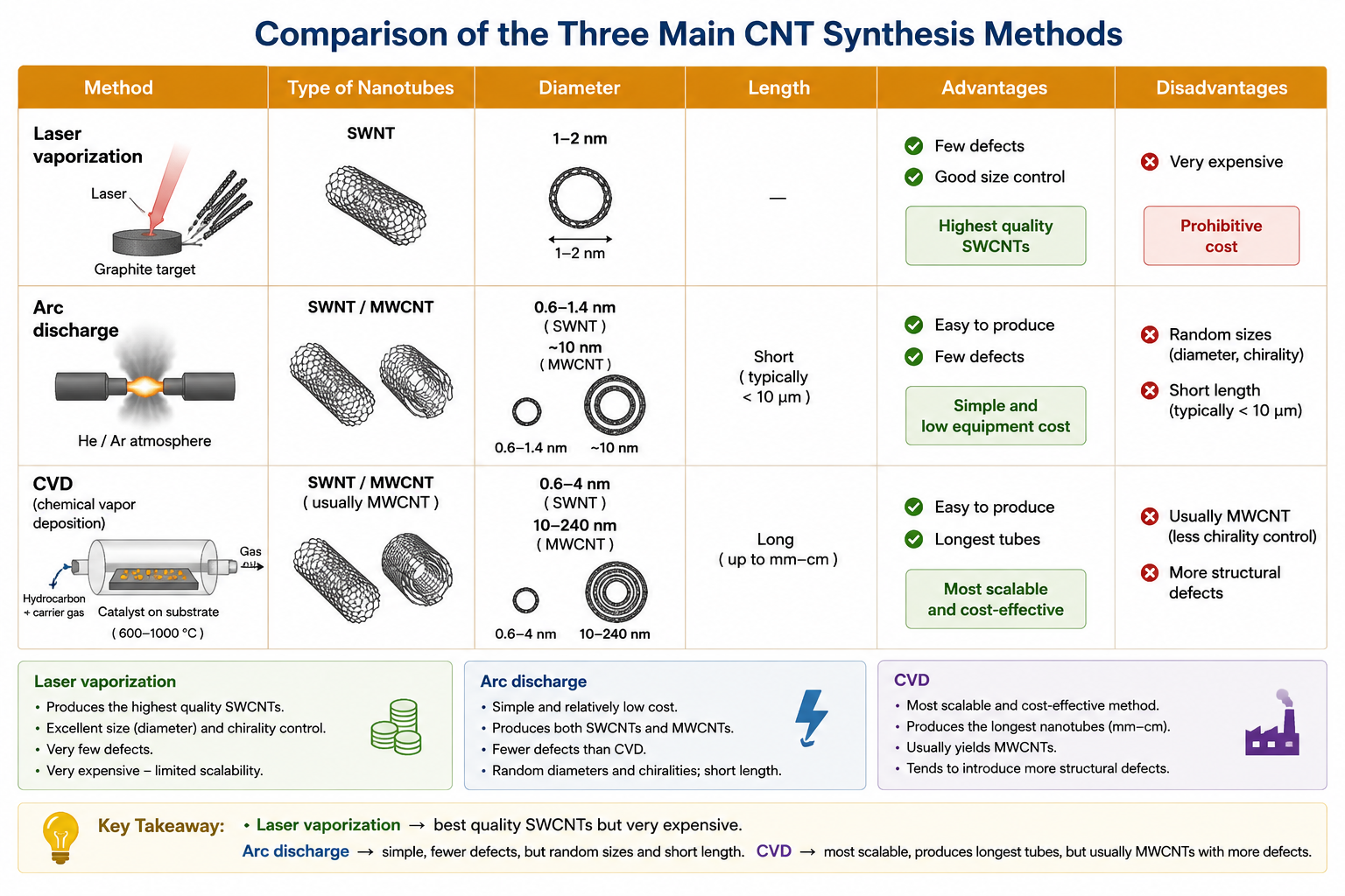
Fig. 28.7 Comparison of the three main CNT synthesis methods. Laser vaporisation gives the highest quality SWCNTs but at prohibitive cost. Arc discharge is simpler and produces fewer defects but gives random sizes. CVD is the most scalable and produces the longest tubes, but tends to yield MWCNTs and introduces more structural defects.
Laser vaporisation fires a pulsed Nd:YAG laser at a graphite target in a furnace at 1200 °C under argon flow. The ablated carbon self-assembles into SWCNTs that collect on a cooled downstream collector as a nanotube felt. It gives the fewest defects and the best diameter control (1–2 nm), but is very expensive and cannot be scaled easily.
Arc discharge passes a high current between two graphite electrodes in a helium atmosphere. The intense arc (>3000 °C) vaporises the anode; the carbon deposits on the cathode and walls as a mixture of SWCNTs, MWCNTs, and amorphous carbon. It produces few defects and the process is straightforward, but yields tubes of random diameter and only short lengths.
Chemical vapour deposition (CVD) decomposes a hydrocarbon gas (methane, ethylene, acetylene) over metal nanoparticle catalysts (Fe, Co, Ni) at 500–1000 °C. The carbon released from the catalyst surface assembles into tubes that grow to lengths of up to hundreds of micrometres. CVD is the most scalable method and the only one currently used industrially, but commonly gives MWCNTs and introduces more defects than the other methods. The key process parameters are temperature and gas pressure.
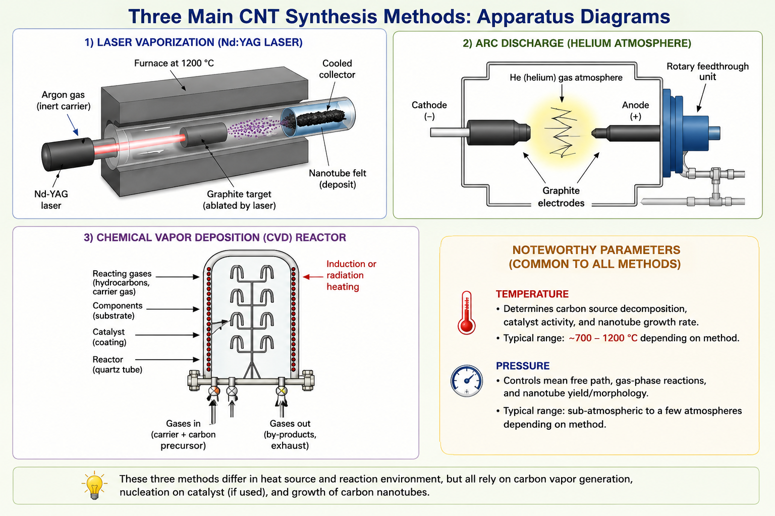
Fig. 28.8 Apparatus diagrams for the three CNT synthesis methods. Top-left: laser vaporisation with Nd:YAG laser and cooled collector. Top-right: arc discharge between graphite electrodes in helium. Bottom: CVD reactor with induction heating and gas flow. Key process parameters common to all three are temperature and pressure.
Common challenges across all three synthesis methods include low yield, high cost, difficulty in controlling the tube diameter, and the production of impurities (amorphous carbon, metal catalyst particles, fullerenes) embedded in the nanotube network. Purification by acid oxidation, gas-phase oxidation, or filtration is typically required, but can itself damage the tube walls or fail to remove large aggregates.
9 Discovery: Iijima and the Arc Discharge Story
The discovery of MWCNTs is attributed to Sumio Iijima at NEC Corporation in 1991, who observed them in the carbon deposit formed by electrical arc discharge between two carbon electrodes — the same process that Kroto and Smalley had used in the 1980s to discover C₆₀ fullerene (buckminsterfullerene). Kroto, Curl, and Smalley had found that under the right arc-discharge conditions, carbon atoms spontaneously self-assemble into C₆₀ cage structures. Iijima recognised that by modifying the arc-discharge conditions, carbon could self-assemble into tubular rather than spherical structures. His identification of the multi-walled tubes required exceptional TEM skill — he measured the discrete nanotube diameters and interlayer spacings directly from high-resolution lattice images and was the first to correctly interpret the contrast in terms of nested graphitic cylinders.
10 CNTs for Nanoelectronic Interconnects
As CMOS transistor dimensions shrink below 10 nm, copper interconnects — the wires that carry signals between transistors — face a fundamental materials limit. Conventional copper wires support current densities up to about 10⁵ A/cm² before electromigration (the physical displacement of copper atoms by the electron wind) causes failure and heating. At interconnect widths below ~20 nm, grain boundary and surface scattering dramatically increase copper resistivity, compounding the problem.
Metallic SWCNTs offer a direct solution: observed current densities of up to 10⁹ A/cm² — four orders of magnitude beyond copper — arise from 1D ballistic transport. Because the electronic states are confined in the directions perpendicular to the tube axis, the only remaining conduction channel runs along the tube axis. The near-complete absence of phonon and impurity scattering perpendicular to the tube makes SWCNTs essentially 1D ballistic conductors at room temperature.
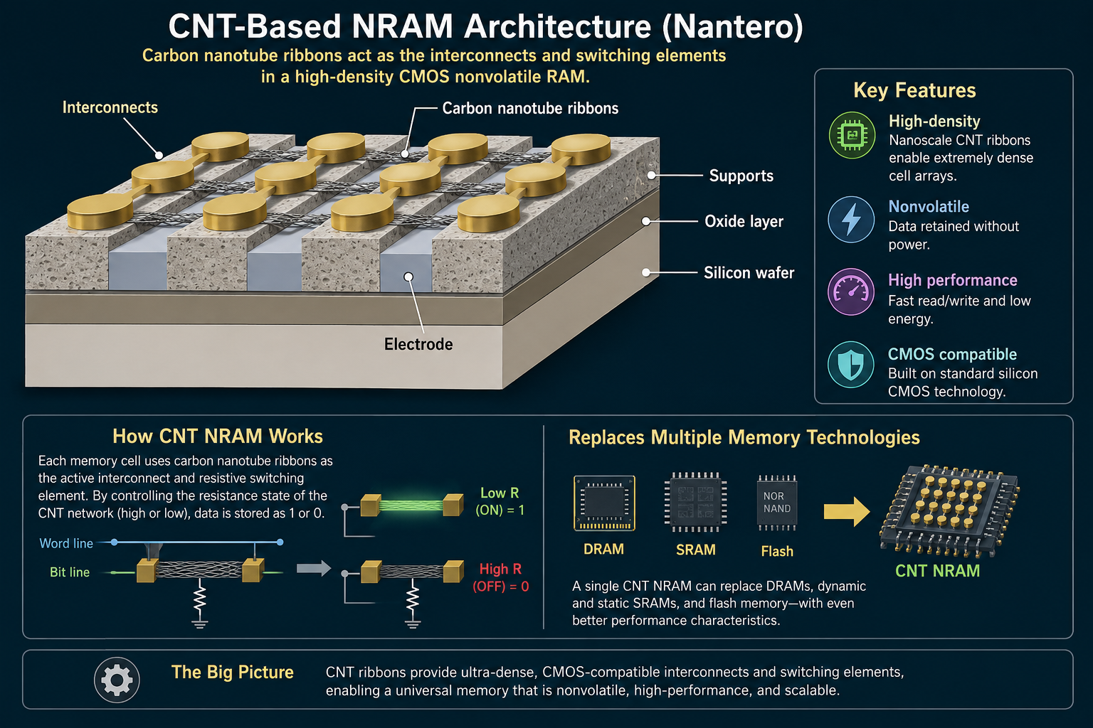
Fig. 28.9 CNT-based NRAM architecture from Nantero. Carbon nanotube ribbons serve as the active interconnect and switching elements in a high-density CMOS nonvolatile RAM capable of replacing DRAM, SRAM, and flash memory. The silicon wafer, oxide layer, and support structure are conventional CMOS components; only the interconnect layer is replaced with CNTs.
11 CNT Composites
CNTs are nearly ideal reinforcement fillers for composite materials: their high aspect ratio (length/diameter up to 10⁶), combined with exceptional stiffness, strength, electrical conductivity, and thermal conductivity, motivates their incorporation into polymer, ceramic, and metal matrices. The driving properties sought are mechanical reinforcement (higher stiffness and fracture toughness), electrical percolation (turning an insulating polymer into a conductor at very low filler loading), and thermal management.
The principal challenges in CNT composites are achieving uniform dispersion without agglomeration, controlling the alignment of tubes within the matrix, engineering the interface between nanotube and matrix for effective load transfer, and managing cost — the high price of purified SWCNTs currently limits their weight fraction to fractions of a percent in most practical formulations.
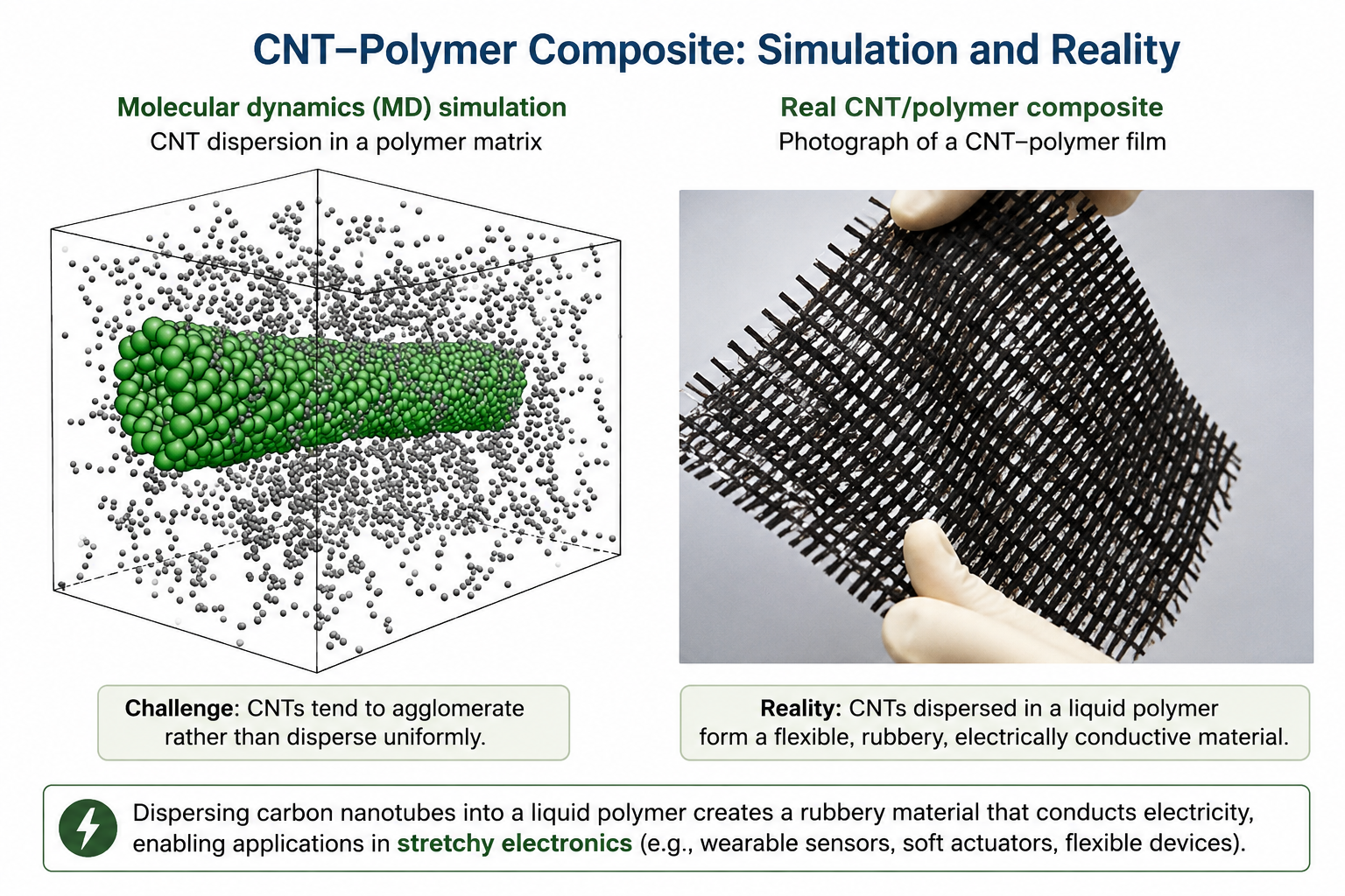
Fig. 28.10 CNT composite: simulation and reality. Left: MD simulation of CNT dispersion in a polymer matrix showing the challenge of achieving uniform distribution (the green CNT is localised in one region). Right: photograph of a CNT/polymer composite — CNTs dispersed in a liquid polymer create a rubbery, electrically conductive material suitable for stretchy electronics applications.
12 Silicon Photolithography: CNT Integration Context
The integration of CNTs into electronic devices ultimately requires patterning them alongside conventional silicon CMOS circuitry. Understanding silicon photolithography — the dominant patterning technology for Si-based devices — is therefore prerequisite to appreciating both the opportunities and the challenges of CNT nanoelectronics.
Photolithography transfers a pattern from a mask to a photosensitive polymer film (photoresist) on a substrate. The process has five steps: (1) Coat — spin-coat the photoresist onto the substrate; (2) Expose — illuminate through the mask with UV light; (3) Develop — dissolve the exposed (positive resist) or unexposed (negative resist) regions; (4) Etch — remove the underlying material not protected by resist; (5) Strip — remove the residual resist.
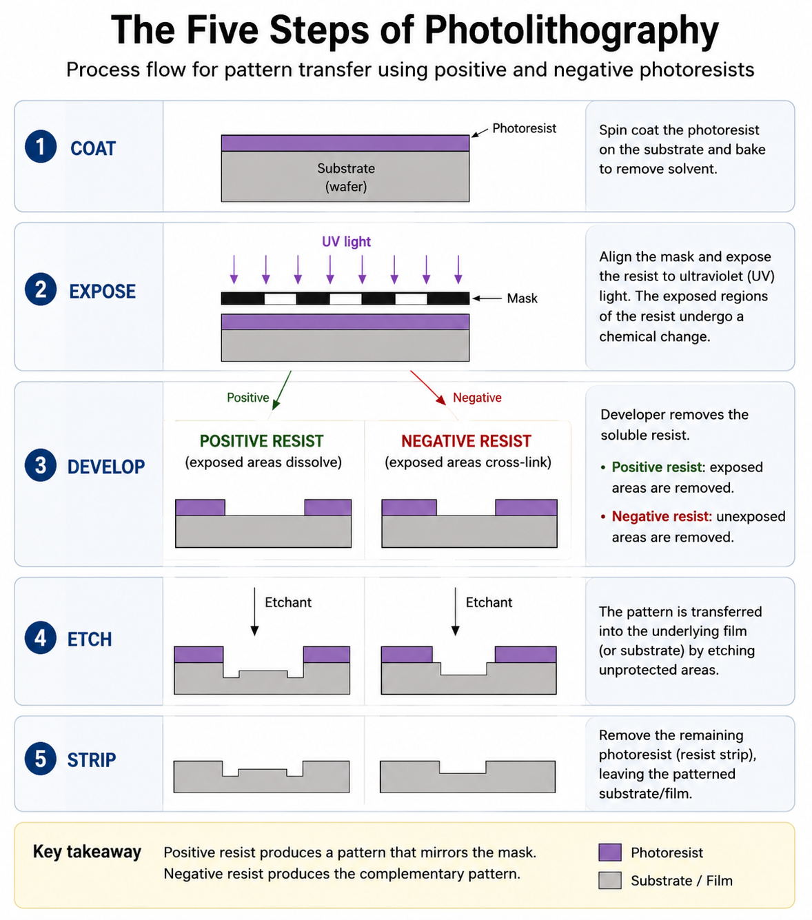
Fig. 28.11 The five steps of photolithography: coat, expose, develop, etch, strip. The positive and negative resist pathways diverge at the develop step: positive resist is dissolved where exposed, leaving a pattern that mirrors the mask; negative resist is cross-linked where exposed and removed where unexposed, giving the complementary pattern.
The choice between positive and negative photoresist depends on the desired pattern geometry and process requirements. In a positive resist, UV exposure changes the chemical structure of the polymer to make it more soluble in the developer — the exposed regions wash away, leaving the unexposed areas as the patterned features. This faithfully replicates the mask. In a negative resist, UV light cross-links the polymer chains, making the exposed regions harder and less soluble — the unexposed regions are removed by the developer, leaving an inverted (negative) image of the mask.
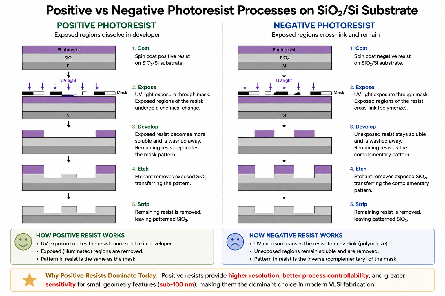
Fig. 28.12 Positive (left) and negative (right) photoresist processes on a SiO₂/Si substrate. In positive resist, the exposed regions dissolve, replicating the mask pattern in the remaining resist; etching then transfers that pattern to SiO₂. In negative resist, the exposed regions cross-link and remain; the complementary (inverted) pattern is transferred. Positive resists now dominate VLSI fabrication because of superior resolution and process controllability for sub-100 nm features.
Negative resists were dominant in early integrated circuit manufacturing. Today, positive resists have become standard in VLSI fabrication because they offer better resolution and greater process controllability for small geometry features, and they avoid the edge-swelling artefacts that arise when cross-linked negative-resist islands swell during development. The resolution limit of conventional UV photolithography is ultimately set by diffraction and is roughly equal to the wavelength of light used (typically 193 nm for ArF excimer laser sources in modern fabs), which requires immersion lithography, phase-shift masks, and multiple-patterning tricks to achieve sub-20 nm feature sizes.
✦ References & Further Reading
- Iijima, S. (1991). Helical microtubules of graphitic carbon. Nature, 354, 56–58. [The original MWCNT discovery paper.]
- Dresselhaus, M. S., Dresselhaus, G., & Avouris, P. (Eds.) (2001). Carbon Nanotubes: Synthesis, Structure, Properties, and Applications. Springer.
- Saito, R., Dresselhaus, G., & Dresselhaus, M. S. (1998). Physical Properties of Carbon Nanotubes. Imperial College Press.
- De Volder, M. F. L. et al. (2013). Carbon nanotubes: present and future commercial applications. Science, 339, 535–539.
- Avouris, P., Chen, Z., & Perebeinos, V. (2007). Carbon-based electronics. Nature Nanotechnology, 2, 605–615.
- Madou, M. J. (2002). Fundamentals of Microfabrication (2nd ed.). CRC Press. [Photolithography and silicon processing.]
Key Takeaways
- CNT geometry is fully specified by the chiral vector (n, m): armchair (n = m) → metallic; zigzag (m = 0) → semiconducting; chiral → metallic when (n − m) mod 3 = 0. MWCNTs are always metallic.
- 1D quantum confinement in a near-perfect sp² lattice yields exceptional stiffness (~1 TPa), current density (~10⁹ A/cm²), and thermal conductivity (~3000–6000 W/mK) via ballistic transport.
- Synthesis routes — laser vaporisation, arc discharge, CVD — trade off tube quality, type selectivity, and cost.
- Applications include nanoelectronic interconnects, polymer composites for stretchy electronics, and structural reinforcement; device integration uses standard silicon photolithography with positive resists.
Applications of Nanomaterials & Quantum Devices
Nanomedicine · Catalysis · Band Gap Engineering · Quantum Wells · Strain Engineering
Contents
Why Nanomaterials Find Applications
The commercial and scientific interest in nanomaterials stems from three broad categories of advantage that nanoscale architecture brings over conventional bulk materials. First, peculiar physical properties emerge at the nanoscale that have no bulk analogue — gold nanoparticles, for instance, catalyse the oxidation of carbon monoxide at room temperature, a reaction that bulk gold is essentially inert to. Second, the enormous surface-area-to-volume ratio of nanostructured materials opens up applications wherever interfacial chemistry drives function: titanium dioxide nanoparticles used in dye-sensitised photochemical solar cells, or metallic nanoparticles deployed as chemical sensors, exploit this principle directly. Third, nanoscale architecture allows multiple functionalities to be co-located within a single structure or device — a property that is especially enabling for biomedical systems where simultaneous sensing, drug delivery, and mechanical manipulation are required.
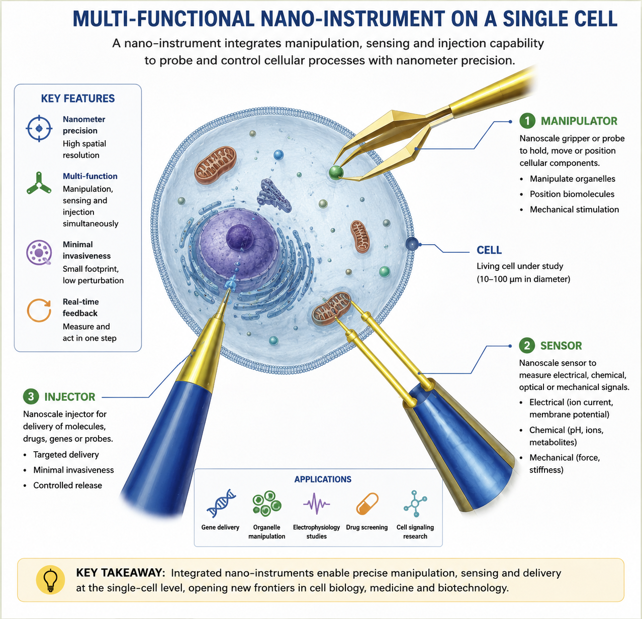
Fig. 29.1 Concept illustration of a multi-functional nano-instrument operating on a single cell: a manipulator probe, a sensor, and an injector can act simultaneously at the cellular level.
Nanomedicine and Nanobots
Perhaps the most ambitious near-term application domain is medicine. The scaling challenges of miniaturisation — instruments small enough to operate at the molecular level inside living tissue, sensors smaller than a single cell capable of monitoring biological processes in real time, and machines capable of neutralising chemical threats or repairing metabolic defects inside the human body — map directly onto the strengths of nanotechnology. Nanobots (nano-scale robotic devices) designed for in vivo use are expected to deliver improved therapy and diagnostics by operating precisely where and when intervention is needed, rather than relying on systemic drug administration.
Key therapeutic capabilities envisaged for nanobots include: delivering therapeutic agents directly to the site of early-stage diseases before symptoms manifest; repairing metabolic or genetic defects at the cellular level; and releasing drugs in a localised area, thereby minimising the side-effects that accompany generalised drug therapy. The molecular imaging and therapy schematic below illustrates this progression — from diagnosing a tumour and targeting medication, to homing on the tumour site and killing cancer cells, while improved imaging tracks outcomes in real time.

Fig. 29.2 Artistic renderings of medical nanobots: (left) a nanobot navigating among red blood cells, operating at cellular scale; (right) a nanobot targeting and neutralising virus particles.

Fig. 29.3 Molecular imaging and therapy pipeline: nanoparticle-based drug carriers allow simultaneous improvement of tumour imaging and localised cancer therapy, reducing systemic side-effects.
A key unresolved challenge for in vivo nanobots is retrieval after use. Residual devices could be eliminated via normal metabolic pathways (metabolism and excretion), which is why biodegradable materials such as calcium phosphate are considered ideal construction materials. The alternative risk — nanobots remaining in the body, clogging biological systems, or malfunctioning — would create new forms of pollution at the cellular scale.
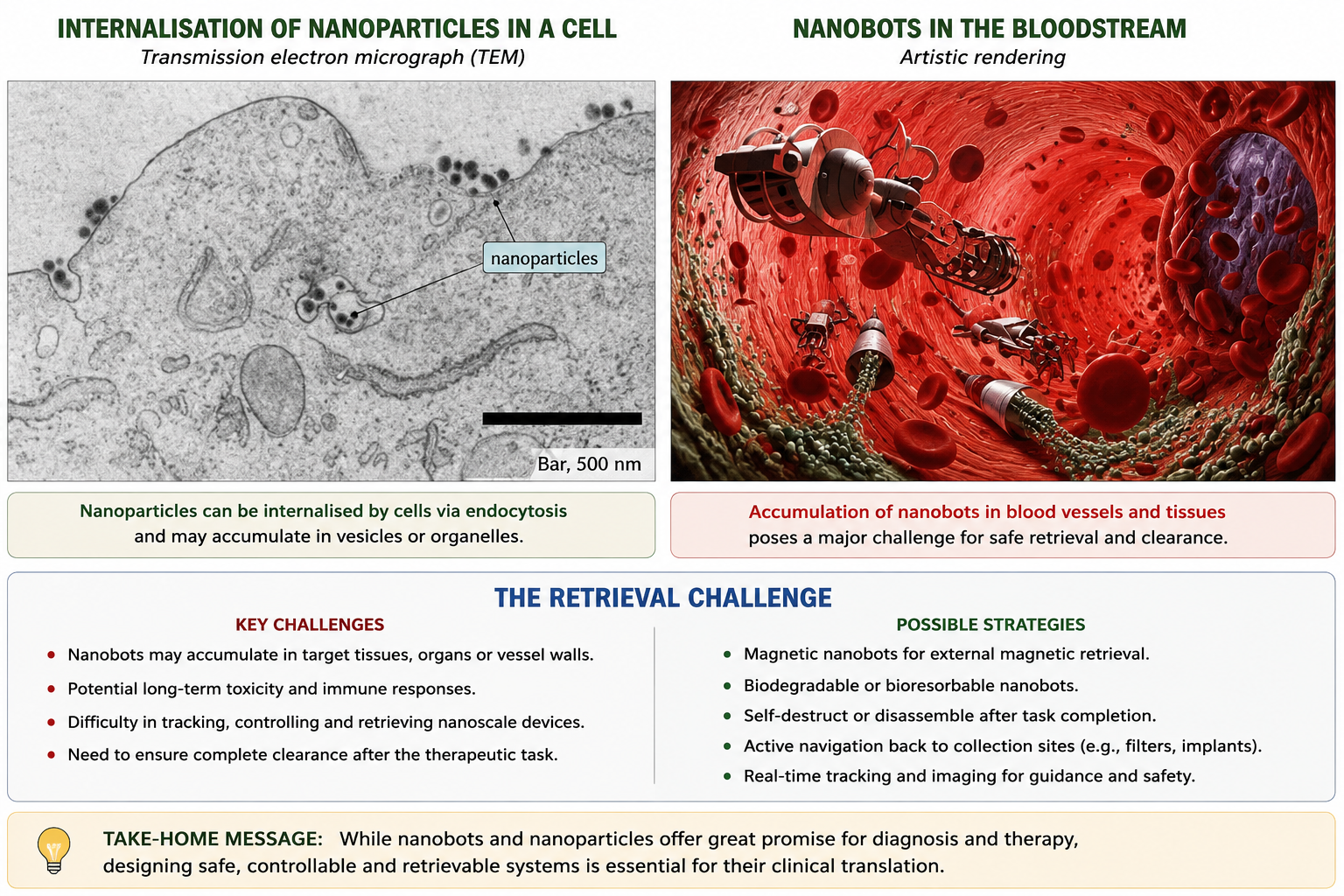
Fig. 29.4 Left: TEM of a cell (500 nm scale bar) showing internalised nanoparticles. Right: artistic rendering of nanobot accumulation in a blood vessel — illustrating the retrieval challenge.
Catalytic Properties: Gold Nanoparticles
Gold is a compelling case study in how nanoscale size changes everything. Bulk gold is chemically inert — it does not oxidise in air, resists most acids, and has little catalytic activity. Nano-gold, however, catalyses the oxidation of CO and the destruction of SO₂ at room temperature, reactions that conventionally require elevated temperatures and specialised platinum-group catalysts. This transformation arises from a combination of size effects and a quantum mechanical phenomenon specific to heavy elements: the relativistic effect.
Gold has the bulk electronic configuration [Xe] 4f¹⁴ 5d¹⁰ 6s¹. In a gold atom, the innermost 1s electrons must travel at a speed approaching 60% of the speed of light to maintain their orbital position around the highly charged nucleus (Z = 79). Special relativity predicts that at such velocities, the electron mass increases, causing the 1s orbital to contract. By orthogonality, all s-orbitals contract in sympathy. This contraction screens the nucleus less effectively, allowing the 5d electrons to be destabilised and move to higher energy — the exposed 5d electrons become the seat of high oxidation and catalytic activity in nano-Au.
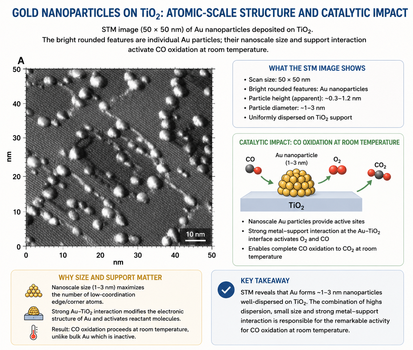
Fig. 29.5 STM image (50 × 50 nm) of Au nanoparticles deposited on TiO₂. The bright rounded features are individual Au particles; their nanoscale size and support interaction activate CO oxidation at room temperature.
At low sizes the relativistic contraction of s-orbitals is amplified because the coordination number of surface atoms is reduced — there are fewer neighbouring atoms to restabilise the electron configuration. As particle size falls below ~5 nm, the combination of (i) the high fraction of surface/edge atoms, (ii) charge transfer at the Au–TiO₂ interface, and (iii) the relativistic destabilisation of the 5d band conspires to make nano-gold an unexpectedly powerful oxidation catalyst.
Band Gap Engineering
The ability to tailor the electronic band gap of a semiconductor — and hence its optical absorption and emission wavelength, carrier transport properties, and threshold behaviour — is the foundation of modern optoelectronics. In nanostructured semiconductors this tailoring is achieved via quantum confinement, and the resulting devices are called quantum devices. The driving motivation is to create unusual electronic transport and optical effects that are not accessible in bulk materials.
In bulk semiconductors, band gap engineering is primarily achieved by choosing alloy compositions (e.g. varying the In/Ga ratio in InGaAs shifts Eg from ~0.35 eV for InAs to ~1.42 eV for GaAs). The schematic below shows how the conduction band alignment changes between two different heterojunction systems (AlAs/GaAs versus InAs/GaSb) — in the GaAs-based system the conduction band dips form quantum wells that confine electrons. The Eg versus k plot (right panel) illustrates the Burstein–Moss shift: Sn doping in In₂O₃ fills the conduction band, shifting the apparent optical gap Eg′ to higher energy relative to the undoped case.
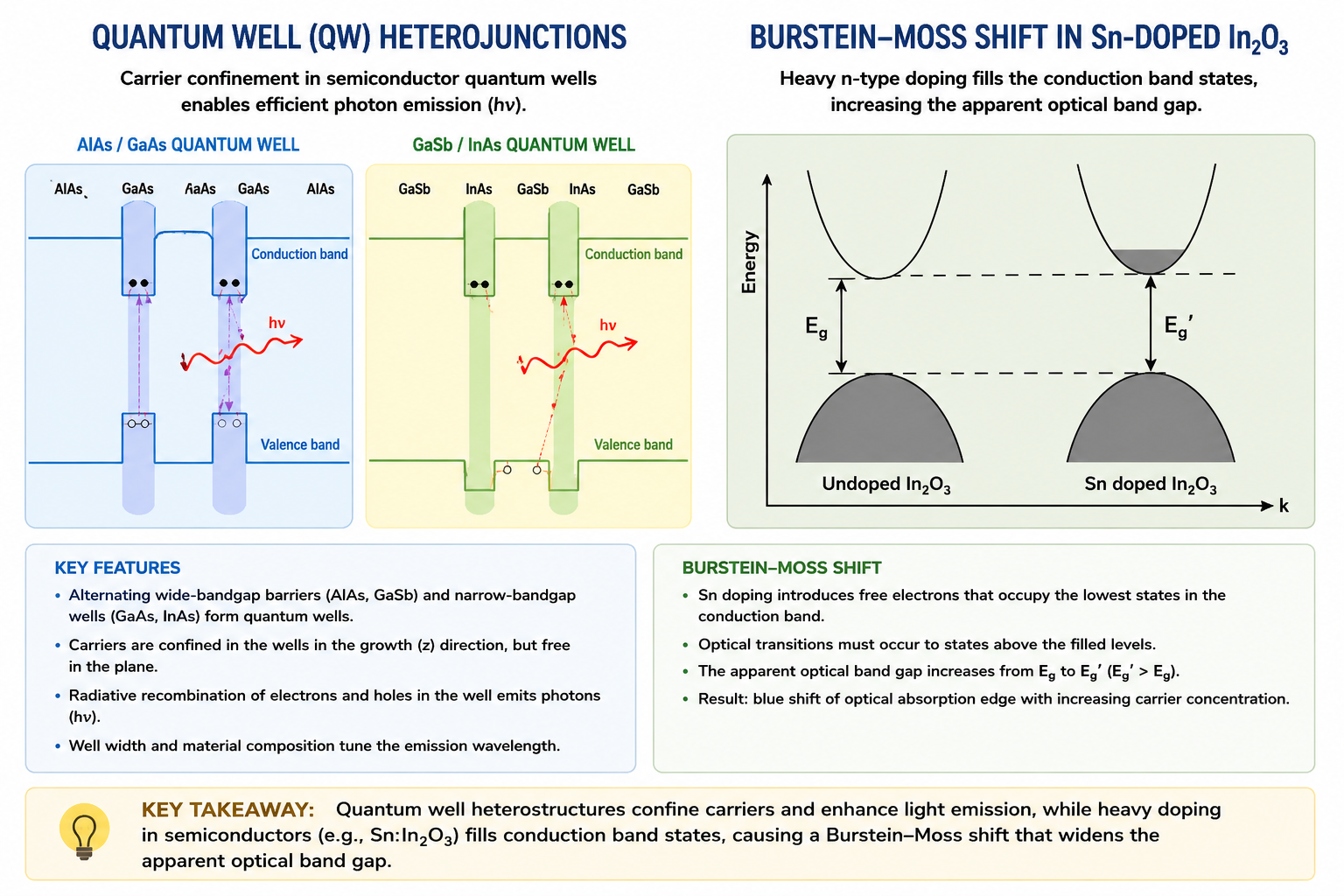
Fig. 29.6 Left: band diagrams of AlAs/GaAs and GaSb/InAs QW heterojunctions showing carrier confinement and photon emission. Right: Burstein–Moss shift in In₂O₃ — Sn doping widens the apparent optical gap Eg′.
Quantum Devices: Single and Multiple Quantum Wells
A quantum well (QW) is a thin layer of lower-band-gap semiconductor sandwiched between higher-band-gap barrier layers — a potential energy well in which carriers are quantum-mechanically confined to discrete energy levels. This confinement changes the density of states from the continuous √E dependence of a bulk 3D semiconductor to a staircase function characteristic of a 2D system, which has profound consequences for laser and LED performance.
Quantum well lasers exhibit improved lower threshold current and lower spectral width compared with bulk active-layer devices. The key parameter distinguishing single QW (SQW) and multiple QW (MQW) designs is the confinement factor Γ — the fraction of the optical mode that overlaps with the active (gain) region. In a single quantum well, Γ is relatively large because all carriers are concentrated in one well. In a multiple quantum well structure, the active region is split across several thin wells separated by barriers, and Γ per well is smaller — but the total gain can be higher because more wells contribute. The net result is higher carrier flow and current densities in single quantum wells (for a given optical mode), but better differential gain and temperature stability in MQW designs.
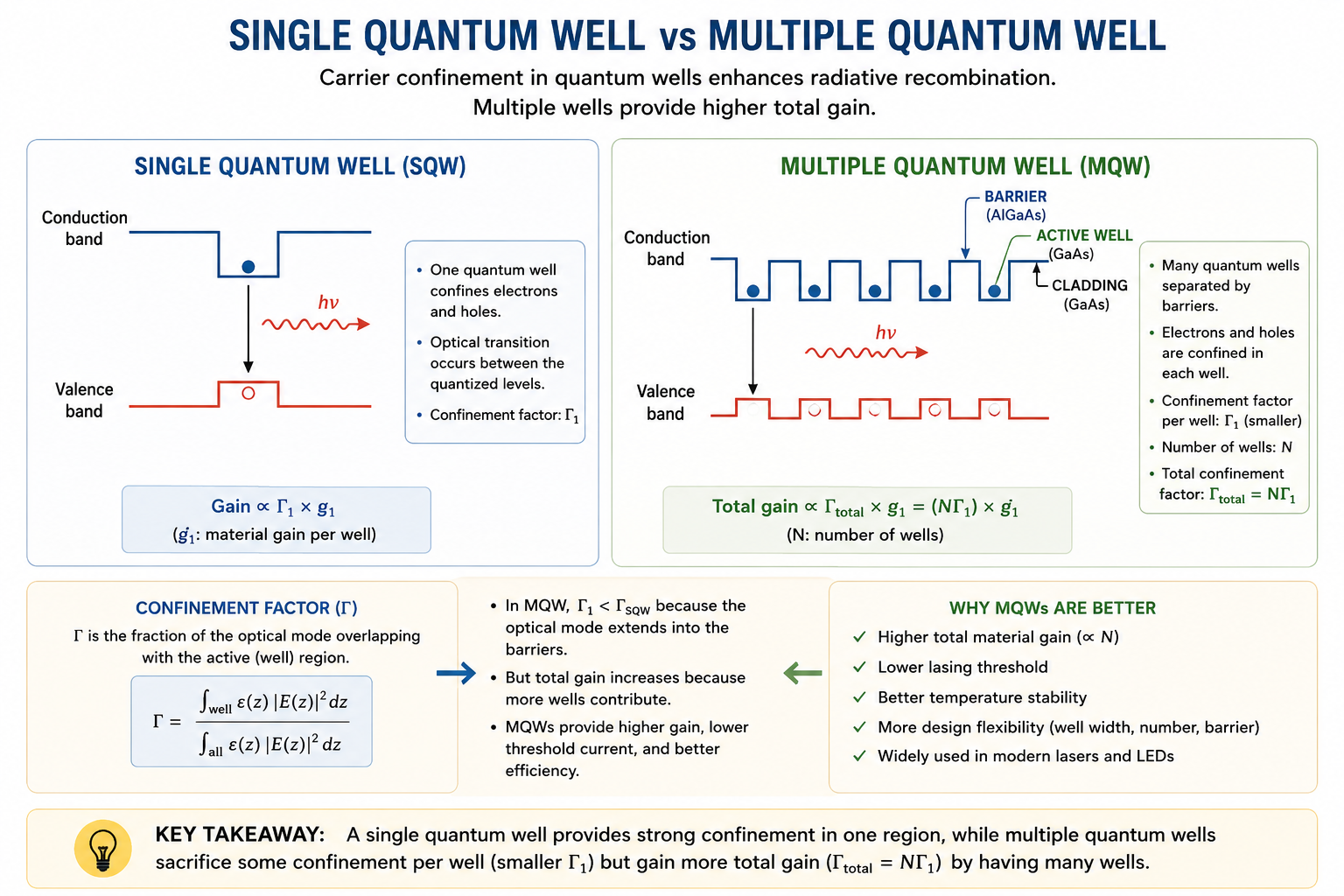
Fig. 29.7 Schematic band diagrams: single quantum well (left) versus multiple quantum well (right). The confinement factor Γ is smaller per well in the MQW but more wells contribute to total gain.
A practical InGaN/GaN MQW LED stack (grown on sapphire) illustrates the full layer architecture. The 6× MQW active region (3 nm wells, 12 nm barriers) is bracketed by an Al₀.₂Ga₀.₈N electron-blocking layer and doped GaN contacts.
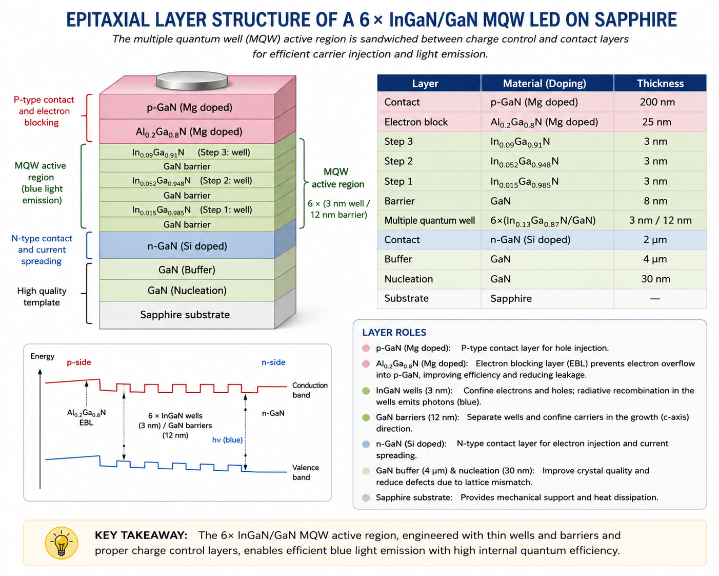
Fig. 29.8 Epitaxial layer stack for a 6× InGaN/GaN MQW LED on sapphire. The MQW active region (3 nm wells / 12 nm GaN barriers) is bracketed by an Al₀.₂Ga₀.₈N electron-blocking layer and doped GaN contact layers.
The confinement factor can be further optimised by moving to a graded-index single quantum well (GRIN-SQW) structure, where the barrier composition is graded continuously from the cladding to the well edge, creating a funnel-shaped potential that improves optical mode overlap. An analogous improvement for MQW structures — the modified multiquantum well (M-MQW) — introduces graded barriers between wells to reduce carrier overflow and improve injection uniformity.

Fig. 29.9 Advanced quantum well architectures: (left) GRIN-SQW — graded barriers improve optical confinement factor; (right) Modified MQW — graded barriers improve carrier injection uniformity across multiple wells.
Material Systems for Band Gap Engineering
The practical material choices for quantum well devices are constrained by lattice constant matching between well and barrier layers (lattice mismatch generates misfit dislocations that degrade performance) and by the desired emission wavelength. The canonical systems are GaAs/AlGaAs (lattice-matched at ~5.65 Å, emitting in the 700–900 nm near-infrared) and InGaAsP/InP or InGaAsN/GaAs (covering the 1.3–1.55 μm telecom windows). The band gap vs. lattice constant plot maps the full space of compound semiconductor options — the rainbow horizontal bands indicate the visible-spectrum wavelengths accessible at each band gap energy.
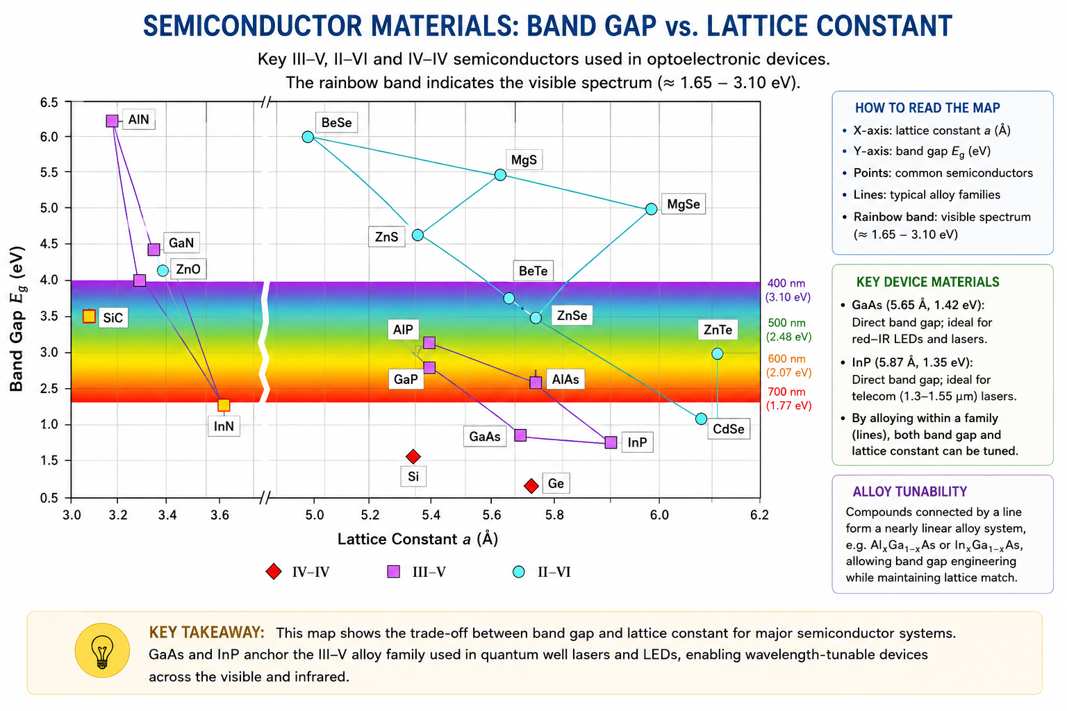
Fig. 29.10 Band gap vs. lattice constant map for III-V, II-VI, and IV-IV semiconductors. The rainbow bands mark visible-spectrum wavelengths. GaAs (5.65 Å, 1.42 eV) and InP (5.87 Å, 1.35 eV) anchor the two principal alloy families for quantum well lasers and LEDs.
Strain Engineering in Compound Semiconductors
When a quantum well layer is grown with a slightly different lattice constant than its barrier, the film is forced to adopt the in-plane lattice constant of the substrate — this introduces biaxial strain in the well. Deliberately engineered strain can alter the valence band structure of the well material, splitting the heavy-hole and light-hole bands and modifying carrier effective masses. The principal benefit is a reduction in Auger recombination — a non-radiative carrier loss mechanism that is especially severe at high carrier densities (as in semiconductor lasers) and at elevated temperatures — yielding better high-temperature laser performance.
The strategy is illustrated by InGaAsN quantum wells grown on GaAs. Compressive InGaAsN-QW layers are alternated with tensile GaAsP or GaAsN barrier layers; the opposing strain states partially cancel (strain compensation), yielding a net reduced strain force in the composite stack. This allows more quantum well periods to be stacked without accumulating dislocations, while simultaneously achieving reduced Auger recombination.
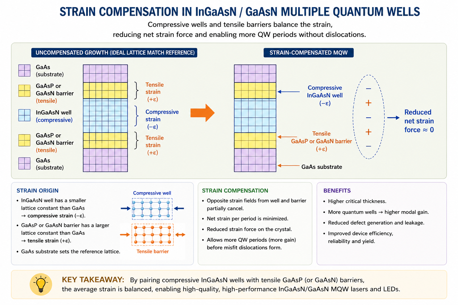
Fig. 29.11 Strain compensation in InGaAsN/GaAsN MQW structures. Compressive InGaAsN wells and tensile GaAsP/GaAsN barriers are combined so that opposing strain fields cancel, reducing net strain force and enabling more QW periods without dislocation formation.
Key Takeaways
- Nanomaterial applications are motivated by three pillars: peculiar physical properties (e.g. nano-Au catalysis via relativistic 5d destabilisation), enormous surface area (sensors, photovoltaics), and multi-functionality (nanobots for localised drug delivery).
- Nanomedicine promises targeted therapy, improved diagnostics, and metabolic repair; engineering challenges include nanobot retrieval and biodegradability.
- Band gap engineering via quantum well design produces practical device architectures (SQW, MQW, GRIN-SQW, M-MQW) with strain-compensated InGaAsN/GaAs structures improving high-temperature laser performance by suppressing Auger recombination.
References
- Haruta, M. (1997). Size- and support-dependency in the catalysis of gold. Catalysis Today, 36(1), 153–166.
- Pyykko, P. & Desclaux, J.P. (1979). Relativity and the periodic system of elements. Accounts of Chemical Research, 12(8), 276–281.
- Chuang, S.L. (2009). Physics of Photonic Devices, 2nd ed. Wiley-Interscience.
- Nakamura, S., Fasol, G. & Pearton, S.J. (2000). The Blue Laser Diode: The Complete Story. Springer.
- Freitas, R.A. Jr. (2005). What is nanomedicine? Nanomedicine: Nanotechnology, Biology and Medicine, 1(1), 2–9.
- Bhattacharya, P. (1997). Semiconductor Optoelectronic Devices, 2nd ed. Prentice Hall.
- IIT Madras NPTEL Nanomaterials Course, Lecture 29 (April 2015).
Broad Applications of Nanomaterials: Electronics, Energy, Magnetics & Safety
Moore's Law · Chip Technology · Energy Harvesting · GMR · Magnetorheological Fluids · Nanotoxicology
Contents
- The Application Landscape of Nanoparticles
- Moore's Law and the Drive to Nanoscale Electronics
- Road Map for Chip Technology
- Nanomaterials in Central Electronic Roles
- Nanomaterials in Energy Applications
- Nanomaterials in the Automotive Sector
- Magnetic Properties: Giant Magnetoresistance
- Magnetorheological Fluids
- Nanotoxicology and Health Safety
- References
The Application Landscape of Nanoparticles
Nanomaterials now permeate virtually every industrial and consumer sector. The map below organises the breadth of nanoparticle applications into eight domains — Textiles, Biomedical, Health Care, Food & Agriculture, Industrial, Electronics, Environment, and Renewable Energy — with specific technologies radiating outward from the central "Nano particles" hub. The sheer range, from anti-stain textiles and self-cleaning glass to quantum computers and MRI contrast agents, reflects the universality of the nanoscale advantage: tunable surface area, size-dependent optical and electronic properties, and the ability to combine multiple functionalities in a single particle.

Fig. 30.1 Applications of nanoparticles across eight major sectors. The radial layout shows how properties such as high surface area, quantum confinement, and tunable chemistry translate into hundreds of distinct technologies.
The breadth extends to consumer products already on the market. Nanotechnology-enhanced products include CNT-reinforced sports equipment (Nanotek aluminium baseball bat, Wilson BLX tennis racket), nano-silver antimicrobial socks (SoleFresh), Pilkington Activ self-cleaning glass, silver wound-care dressings (CURAD), and nano-particle-containing paints and cosmetics — spanning domains from sport to healthcare to construction.

Fig. 30.2 A selection of commercially available nanotechnology-enhanced products: CNT-reinforced sports equipment, nano-silver antimicrobial textiles, self-cleaning glass, silver wound dressings, and nano-containing paints — all already in the consumer market by 2015.
Moore's Law and the Drive to Nanoscale Electronics
Gordon Moore observed in 1965 that the number of transistors on an integrated circuit doubles approximately every two years. The infographic below visualises the scale of this progression: the Intel 4004 (1970) contained 2,300 transistors — fitting into a music hall. By 1980 the Intel 286 held 134,000 — a large stadium. The Pentium III (2000) carried 32 million — the population of Tokyo. By 2011 the Core i7 Extreme Edition packed 1.3 billion transistors — the population of China. Moore's Law thus represents one of history's most sustained engineering exponentials, and it is the primary driver behind the push to nanoscale device fabrication.

Fig. 30.3 Moore's Law visualised: transistor counts per chip have grown from 2,300 (Intel 4004, 1970) to 1.3 billion (Core i7 Extreme, 2011), scaling from a music hall to the entire population of China — all in 40 years.
Road Map for Chip Technology
The semiconductor industry road map charts the progression of transistor architectures from the 100 nm node toward the 2 nm regime, with nanotechnology playing an increasingly central role at each step. The road map moves through several generations: bulk complementary metal-oxide semiconductor (CMOS) devices are followed by fully depleted silicon-on-insulator (FD-SOI) CMOS, then strained silicon, then double-gate CMOS and Ge/Si heterostructures. As feature sizes shrink below ~20 nm, conventional CMOS gives way to nanowire/nanotube self-assembly, 3D integrated circuits (water bonding, crystallisation), and optical interconnects (detectors, lasers, modulators, waveguides). At the frontier — the 2 nm end — are molecular devices, single-electron transistors, and spin devices, where quantum mechanical effects dominate.
Nanowires in particular have potential in high-density data storage (magnetic read heads, patterned media), metallic interconnects for nanoelectronic circuits, and opto-electronic quantum devices — roles that conventional scaled CMOS cannot fulfil.
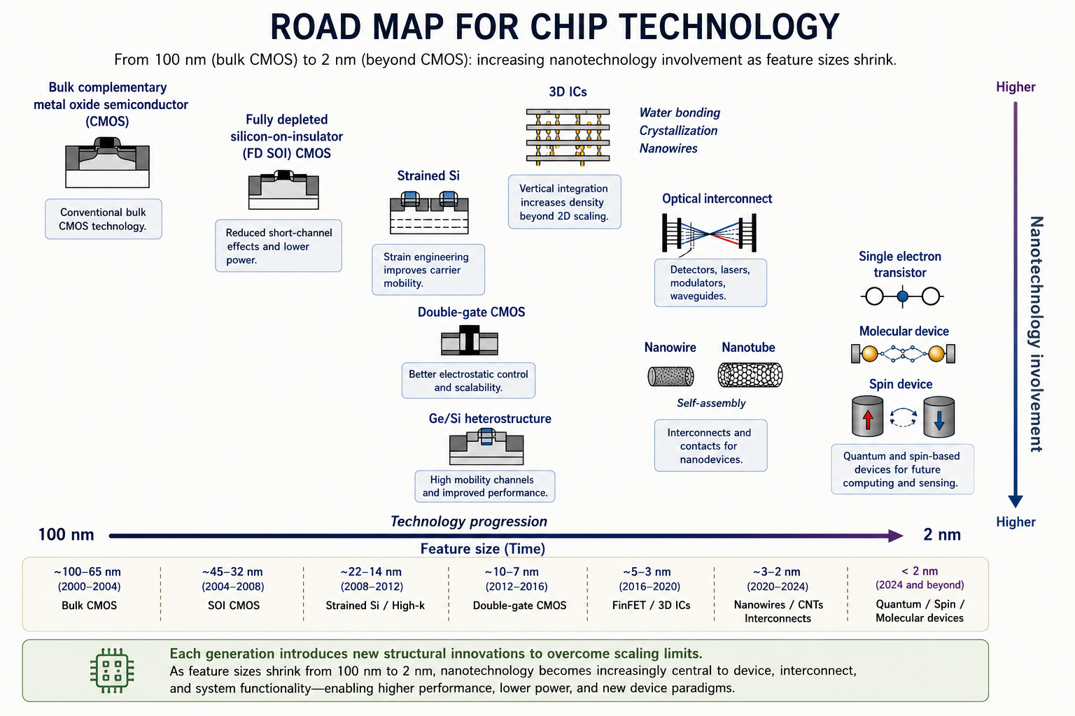
Fig. 30.4 Semiconductor road map from 100 nm (bulk CMOS) to 2 nm (single-electron transistors, molecular devices, spin devices). Each generation introduces a new structural innovation; nanotechnology involvement increases monotonically as feature sizes shrink.
Nanomaterials in Central Electronic Roles
At the circuit level, nanomaterials fill four essential roles: as the active semiconductor channel, as memory units, as interconnects, and as contacts to active devices. The MeRAM (Magnetoelectric RAM) developed by the UCLA team illustrates the memory role: the chip photograph shows a spiral inductor coil on a millimetre-scale die, while the cross-sectional TEM inset (50 nm scale bar) reveals the tri-layer stack — Fixed Layer / Oxide / Free Layer — that constitutes a single magnetic memory bit written by an electric field rather than a current. This approach reduces write energy by orders of magnitude relative to conventional MRAM.
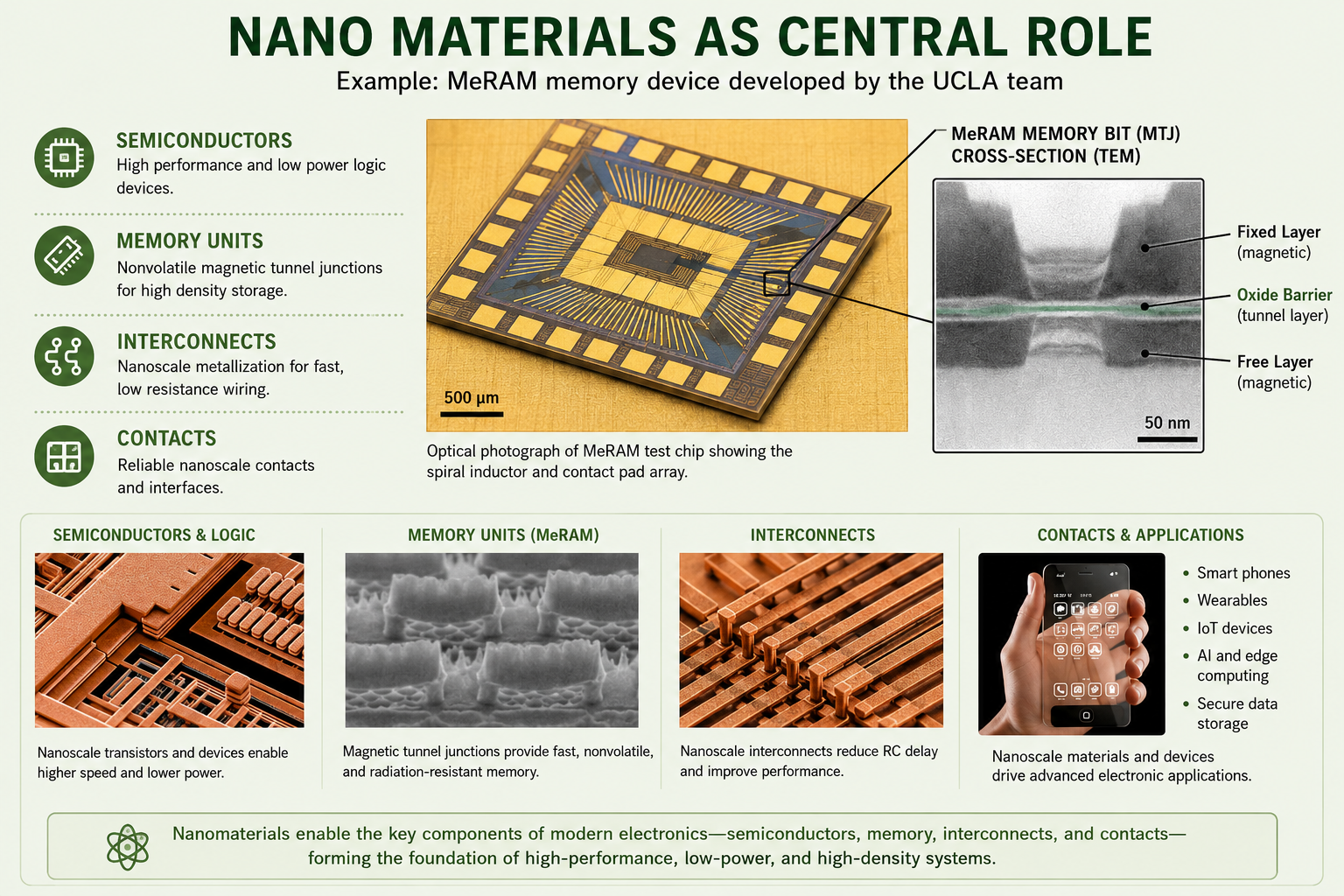
Fig. 30.5 MeRAM memory device (UCLA). Left: optical photograph of the test chip with spiral inductor and contact array. Right inset: TEM cross-section (50 nm scale bar) of the Fixed Layer / Oxide / Free Layer magnetic tunnel junction — the active memory element.
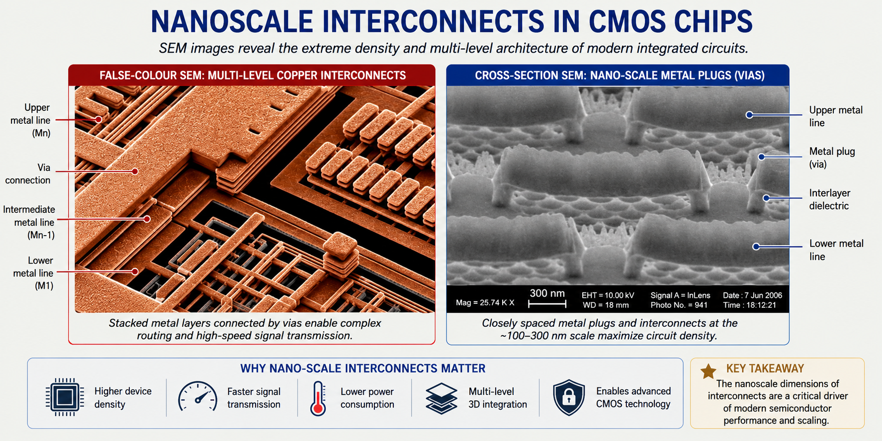
Fig. 30.6 SEM images of nanoscale interconnect structures in CMOS chips. Left: false-colour SEM showing multi-level copper interconnect lines and vias. Right: cross-section SEM (300 nm scale bar) of closely spaced metal plugs — the density of these structures drives the push to nanoscale fabrication.
Making reliable contacts to nanoscale devices — whether carbon nanotubes or semiconductor nanowires — is a critical unsolved engineering challenge. Contacts fall into two categories: end-bonded contacts, where the metal bonds directly to the tube/wire terminus, and side contacts, where the metal electrode overlaps the side of the nanowire. The TEM image (panel a) shows a 1.3 nm diameter CNT with 5 nm scale bar end contacts; panel b shows the atomic model of a CNT with cyan metal atoms capping both ends. The NiSi/Si nanowire cross-section (panel c) shows how a silicide contact forms epitaxially inside the Si nanowire surrounded by SiO₂. The schematic (panel d) generalises this as a Metal–Nanowire end contact. For side contacts (panels e, f): the SEM (panel e, 500 nm scale bar) shows four parallel nanowires with lithographically defined metal side-contact bridges; panel f shows a rendered model of a carbon nanotube resting on a metallic substrate — the prototypical side-contact geometry.
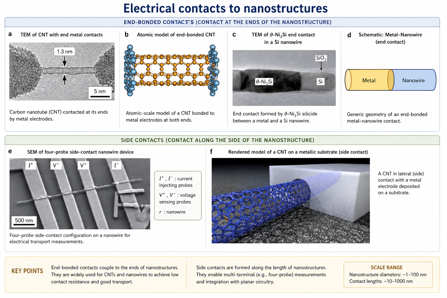
Fig. 30.7 Electrical contacts to nanostructures. Top row (end-bonded contacts): (a) TEM of CNT with end metal contacts; (b) atomic model; (c) TEM of θ-Ni₂Si silicide end contact in a Si nanowire; (d) schematic Metal–Nanowire geometry. Bottom row (side contacts): (e) SEM of four-probe side-contact nanowire device (500 nm scale bar); (f) rendered model of a CNT on a metallic substrate.
Nanomaterials in Energy Applications
The renewable energy sector offers some of the most impactful near-term applications of nanomaterials, exploiting high surface areas and tunable optical properties across three key device types.
Nanostructured photovoltaics take three forms: (a) flexible polymer-based photovoltaics, where semiconductor nanoparticles are embedded in a polymer matrix that can be deposited on flexible substrates; (b) nanoparticle solar cells, where Ag or Au nanoparticles on a p-Si/n-Si junction enhance light absorption through plasmonic scattering; and (c) sprayable self-assembling photocells, where colloidal nanoparticle inks are directly air-brushed onto a substrate to form a solar cell in situ. The schematic below shows the nanoparticle solar cell architecture: incident photons (hν) strike the top aluminium electrode embedded with metal nanoparticles, which scatter and concentrate light into the p-Si active layer above the n-Si base, generating a photocurrent measured across impedance Z.
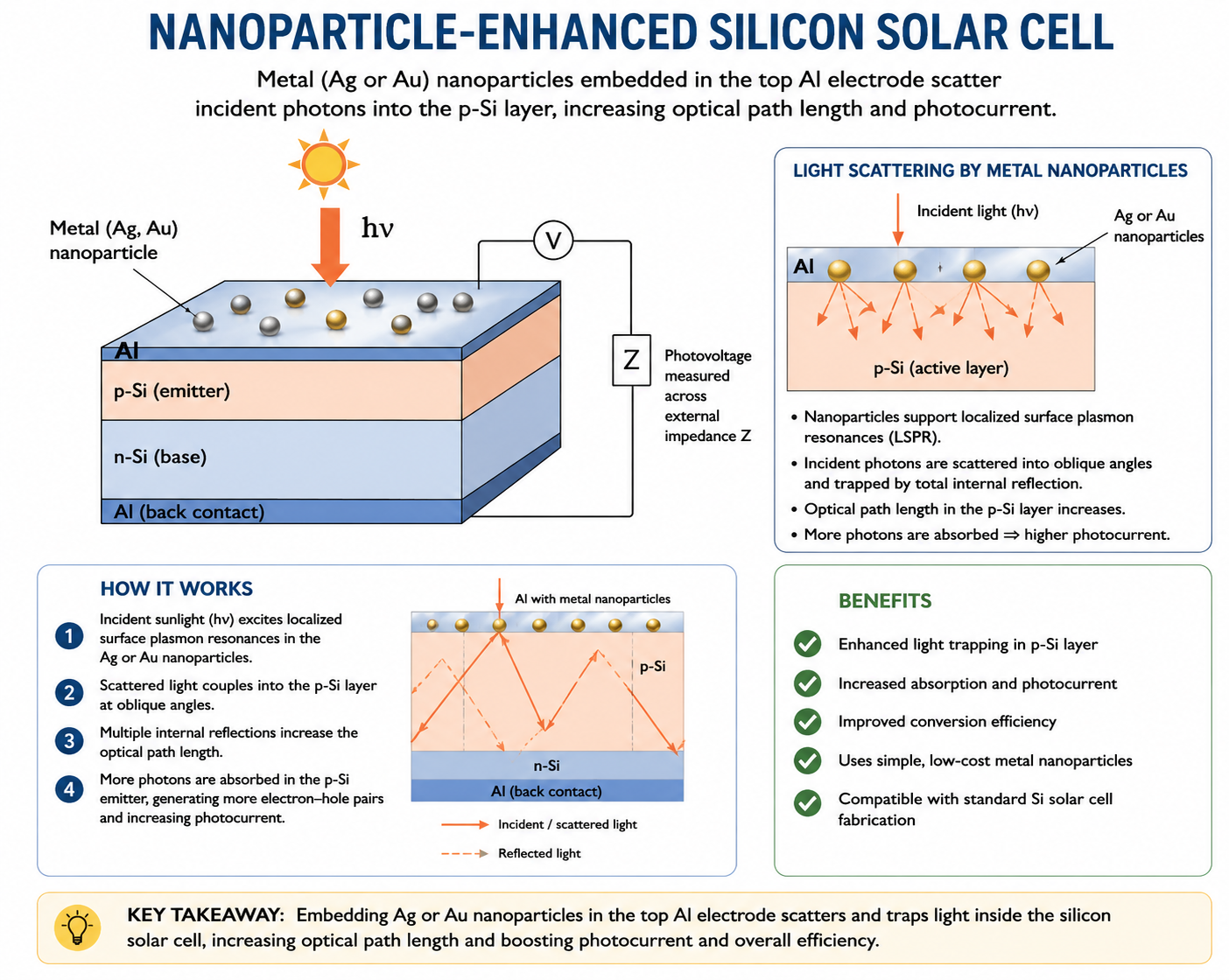
Fig. 30.8 Nanoparticle-enhanced silicon solar cell. Ag or Au nanoparticles embedded in the top Al electrode scatter incident photons into the p-Si active layer, increasing optical path length and photocurrent. Photovoltage is measured across external impedance Z.
Core-shell nanoparticles address both energy and catalysis applications. The Pd/FePt core-shell system shown uses a monolayer-protected FePt nanoparticle array (20 nm scale bar) as an electrocatalyst for water splitting: 2H⁺ + ½O₂ → H₂O in the anodic half-reaction. The kinetics graph on the right shows that the Ni₀.₉₅Ir₀.₀₅ catalyst (with CTAB surfactant, black circles) greatly accelerates hydrazine decomposition (N₂H₄ → N₂ + 2H₂) relative to the unsurfactant-stabilised version (red circles) — a 3× improvement in H₂ production rate over 1200 minutes at room temperature. Nano-phosphate lithium-ion batteries — commercialised under the "NANO Technology" brand — exploit the large surface area of LiFePO₄ nanoparticles to enable faster charge/discharge rates than conventional Li-ion cells, with improved thermal stability.
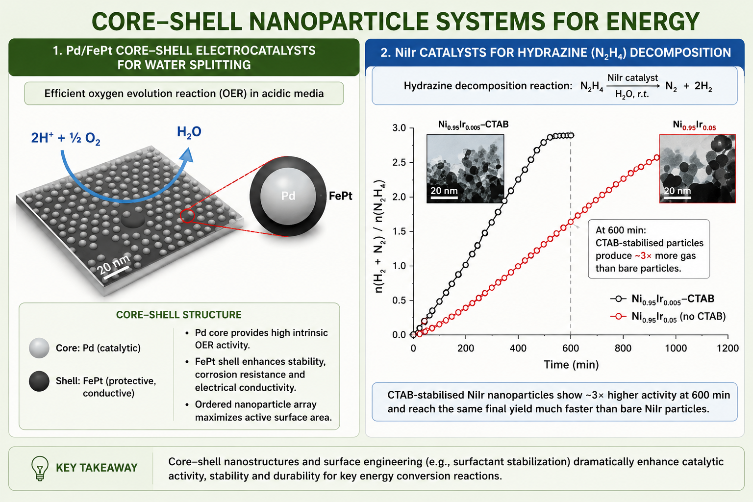
Fig. 30.9 Core-shell nanoparticle systems for energy. Left: Pd/FePt core-shell electrocatalyst array for water splitting (20 nm scale bar). Right: catalytic decomposition of N₂H₄ by NiIr catalyst — CTAB-stabilised particles (black) outperform bare particles (red) by ~3× at 600 min.
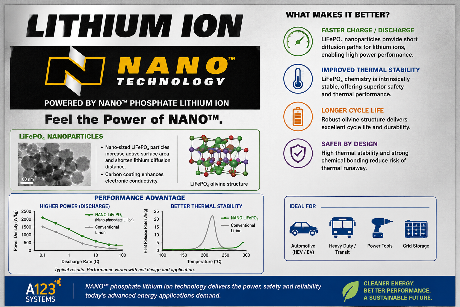
Fig. 30.10 Commercial nano-phosphate lithium-ion battery (A123 Systems / NANO Technology brand). LiFePO₄ nanoparticles enable faster charge/discharge rates and improved thermal stability compared with conventional Li-ion cells.
During the day, solar panels convert sunlight to electricity. This electricity drives an electrolyser that splits water into hydrogen (stored as solar energy) and oxygen. At night, the stored hydrogen is fed into a fuel cell along with atmospheric oxygen; the fuel cell generates electricity and the only byproduct is water — a closed cycle. Nanotechnology improves both steps: nanostructured photocatalysts enhance solar-to-hydrogen efficiency, while nanostructured fuel cell electrodes (e.g. Pt nanoparticles on carbon supports) reduce platinum loading while maintaining high catalytic activity.
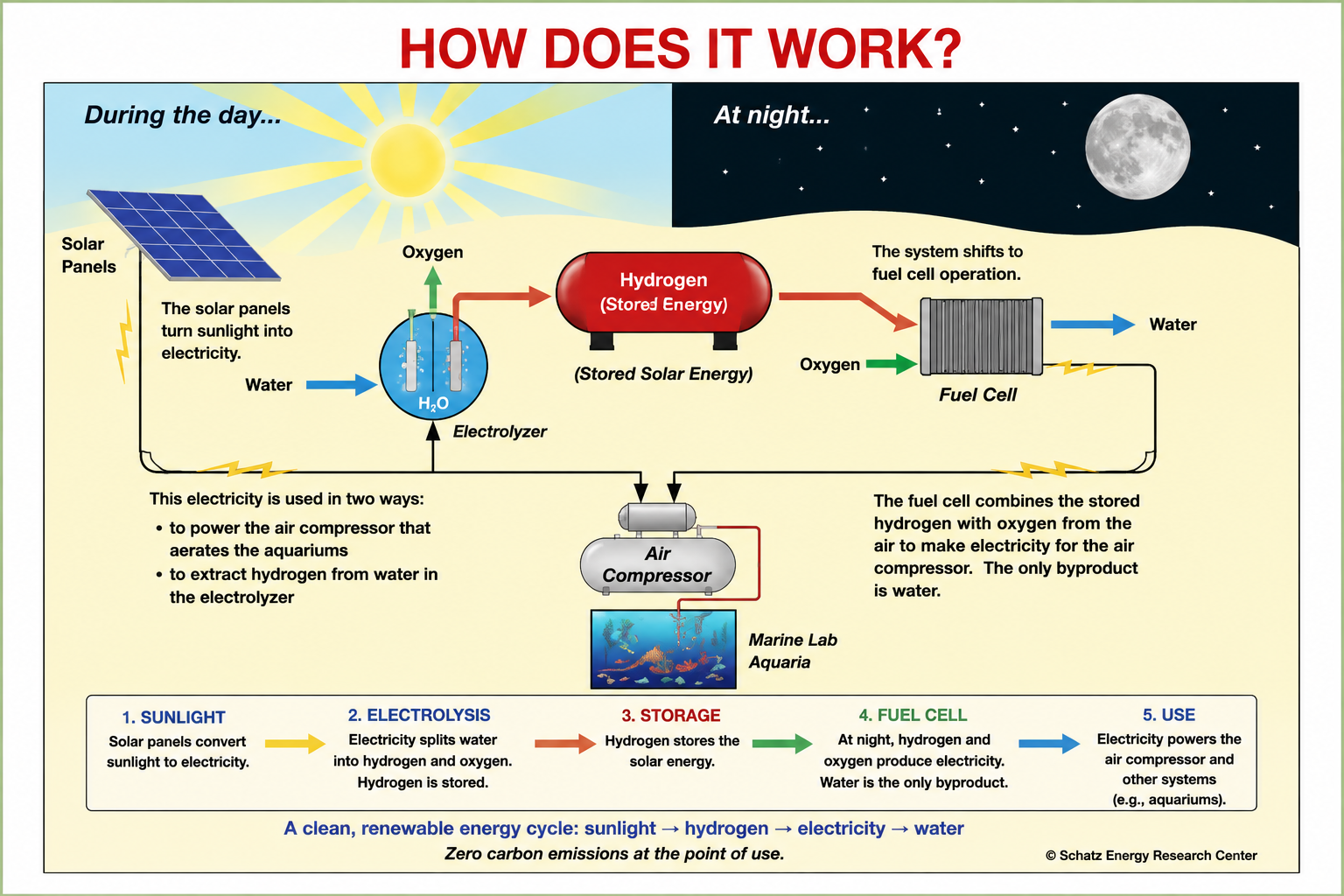
Fig. 30.11 Solar-hydrogen-fuel cell energy cycle (Schatz Energy Research Center). Daytime solar electricity splits water via electrolysis; hydrogen is stored. At night, the fuel cell recombines hydrogen and oxygen to produce electricity — water is the only byproduct.
Nanomaterials in the Automotive Sector
Automotive applications span mechanical, geometric, electronic/magnetic, optical, and chemical functionality categories, with nanomaterials enabling both incremental improvements (existing applications, shown in orange in the table) and transformative new capabilities (possible future applications, shown in yellow). Key entries include: nano varnish and polymer glazing for car body shell hardness and scratch resistance; nanosteel for body structural lightweighting; carbon black nanoparticles in tyres (existing, decades-old); nano filters and gecko-effect coatings for interior air quality; GMR sensors and solar cells in electrics/electronics; and fuel additives and catalysts in the drive train. The table provides a comprehensive cross-reference of which nanomaterial functionality type (mechanical, geometric, electronic/magnetic, optical, chemical) maps onto which vehicle subsystem.

Fig. 30.12 Nanotechnology applications matrix for the automotive sector. Orange cells indicate existing commercial applications; yellow cells indicate possible future applications. Each row is a functionality type; each column is a vehicle subsystem.
Magnetic Properties: Giant Magnetoresistance
The Giant Magnetoresistance (GMR) effect is the dramatic decrease in electrical resistance that occurs when a multilayer structure of alternating ferromagnetic and non-magnetic conductive layers is exposed to an external magnetic field. In the absence of an applied field, adjacent ferromagnetic layers have antiparallel magnetisation (spins oppose), which scatters conduction electrons strongly — giving high resistance. When a magnetic field aligns all layers into parallel magnetisation, scattering is suppressed and resistance drops sharply. The resistance ratio R/R(H=0) can fall by ~80% at fields of a few kGauss, as shown in the Fe/Cr multilayer data (three Cr spacer thicknesses: 1.8 nm, 1.2 nm, 0.9 nm), with the thinnest Cr spacer giving the largest GMR response.
This effect has wide application in magnetic reading heads for computer hard discs and in position sensors. The widely accepted materials system is Cu/Co nanoscale composites, though Fe/Cr was the original discovery system (Albert Fert and Peter Grünberg, Nobel Prize 2007). The effect enabled the areal density of hard drives to increase by over 1000× between 1990 and 2005.
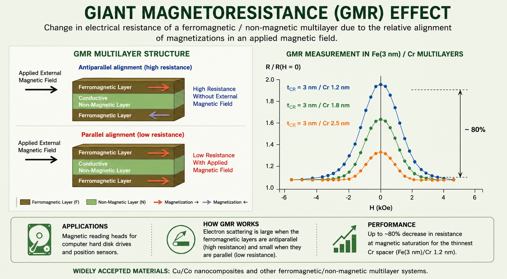
Fig. 30.13 Giant Magnetoresistance (GMR) effect. Left: schematic of ferromagnetic/non-magnetic multilayer showing antiparallel (high resistance) vs. parallel (low resistance) magnetisation states. Right: R/R(H=0) vs. H data for Fe(3nm)/Cr multilayers — up to ~80% resistance decrease at saturation for the thinnest Cr spacer.
Magnetorheological Fluids
Magnetorheological (MR) fluids are suspensions of micron-to-nanoscale ferromagnetic particles (typically iron, ~1–10 μm) in a carrier oil. In the absence of a magnetic field the particles are randomly distributed and the fluid behaves as a low-viscosity liquid (panel a). When a magnetic field is applied perpendicular to the flow direction, the particles align into chain-like columns parallel to the field (panel b), dramatically increasing the fluid's apparent viscosity — the fluid can transition from near-liquid to near-solid within milliseconds. This field-controllable rheology is exploited in controllable dampers for automotive suspensions, seismic building isolation, and prosthetic limbs.
The hardware structure of an MR fluid damper consists of an accumulator, diaphragm, electromagnetic coil, the MR fluid itself, and output wires — all in a sealed cylinder. The working principle is straightforward: input current (magnetic field) controls the MR fluid's yield stress, which determines the generated damping force and resulting displacement/velocity output.

Fig. 30.14 Magnetorheological fluid and damper. (a) Without field: particles distributed randomly, low viscosity. (b) With field: particles chain into columns, high viscosity. Hardware cross-section and working principle schematic of an MR damper showing field-controlled force generation.
Nanotoxicology and Health Safety
The same properties that make nanoparticles useful — small size, high surface area, ability to penetrate biological barriers — also raise legitimate toxicological concerns. Nanoparticles can enter the body via three main routes: inhalation (the most studied route), ingestion, and skin contact or orthopedic implant wear debris. Once inside the body they interact with cells at the organelle level — potentially entering the nucleus, mitochondria, cytoplasm, and lipid vesicles.
The toxicological map below (Buzea, Pacheco, & Robbie, Biointerphases 2007) summarises organ-system-level diseases associated with nanoparticle exposure by entry route. Inhalation leads nanoparticles into the lungs (asthma, bronchitis, emphysema, cancer) and from there into the circulatory system (atherosclerosis, vasoconstriction, thrombosis, high blood pressure), the heart (arrhythmia, heart disease, death), and via olfactory nerves to the brain (Parkinson's, Alzheimer's). Ingestion affects the gastro-intestinal system (Crohn's disease, colon cancer) and other organs. Orthopedic wear particles can cause auto-immune diseases, dermatitis, urticaria, and vasculitis.
Moisturising creams have long incorporated liposomes that enter skin cells to deliver active ingredients. More controversially, nanoscale zinc oxide particles are used in sunblocks to absorb UV light while remaining invisible (unlike micron-scale ZnO which appears white). Although this is effective at UV attenuation, many experts consider it risky because the biological fate of skin-penetrating ZnO nanoparticles — and their potential absorption into the bloodstream — is not yet fully characterised.

Fig. 30.15 Diseases associated with nanoparticle exposure (Buzea et al., 2007). Entry routes (inhalation, ingestion, orthopedic wear debris) lead to distinct organ-system pathologies. Inhalation has the broadest systemic reach, potentially affecting lungs, cardiovascular system, and brain.
Key Takeaways
- Electronics scaling follows Moore's Law; the road map progresses from 100 nm CMOS through strained Si and FD-SOI toward 2 nm molecular/spin devices.
- Energy applications include plasmonic nanoparticle photovoltaics, core-shell electrocatalysts for water splitting, and nano-phosphate lithium-ion batteries.
- Automotive benefits encompass nano varnishes, nanosteel, GMR sensors for read heads and position sensing, and magnetorheological fluid dampers for prosthetics and vehicles.
- Nanotoxicology is the necessary counterweight: the same properties — small size, high surface area, biological penetration — that enable these applications carry inherent risks requiring characterisation and regulation.
References
- Buzea, C., Pacheco, I.I. & Robbie, K. (2007). Nanomaterials and nanoparticles: Sources and toxicity. Biointerphases, 2(4), MR17–MR71.
- Fert, A. (2008). Nobel Lecture: Origin, development, and future of spintronics. Reviews of Modern Physics, 80(4), 1517–1530.
- Baibich, M.N. et al. (1988). Giant magnetoresistance of (001)Fe/(001)Cr magnetic superlattices. Physical Review Letters, 61(21), 2472–2475.
- Rabinow, J. (1948). The magnetic fluid clutch. AIEE Transactions, 67, 1308–1315.
- Pillai, S. et al. (2007). Surface plasmon enhanced silicon solar cells. Journal of Applied Physics, 101, 093105.
- Tanaka, S. et al. (2008). MeRAM: Magnetoelectric RAM for low-power embedded memory. IEEE IEDM.
- IIT Madras NPTEL Nanomaterials Course, Lecture 30 (April 2015).